Six of the seven grand challenges identified focus on the following: developing metrology for materials purity and properties; future microelectronics manufacturing; advanced packaging to integrate separately manufactured components; enhancing the security of devices across the supply chain; improving tools for modeling and simulating Semiconductor materials, designs and components; and improving the manufacturing process. The final challenge highlights the need for standardising new materials, processes and equipment

“We’ve received extensive feedback from stakeholders across industry, academia and government that will help us provide urgently needed measurement services, standards, manufacturing methods and test beds,” says NIST director Laurie Locascio.
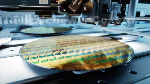
NIST is the only national laboratory dedicated to measurement science, or metrology, and the recently enacted CHIPS and Science Act calls on NIST to conduct critical metrology research and development (R&D) in support of the domestic semiconductor industry to enable advances and breakthroughs for next-generation microelectronics.
Metrology is needed at all stages of semiconductor technology development, from basic and applied R&D in the laboratory to demonstrating proof of concept, prototyping at scale, factory fabrication, assembly and packaging, and performance verification prior to final deployment.
The report released today draws on input received through a series of Semiconductor Metrology Workshops convened by NIST that brought together more than 800 participants from industry, academia and government. Input was also gathered through a Department of Commerce Request for Information and direct feedback from industry.
The report is at:
“Strategic Opportunities for U.S. Semiconductor Manufacturing: Facilitating U.S. Leadership and Competitiveness through Advancements in Measurements and Standards” can