
The same team, from IBS’s Center for Multidimensional Carbon Materials (CMCM), had previously reported single-crystal adlayer-free films of graphene, but they always contained long folds (see diagram) that form from tall wrinkles as the graphene cooled after growth.
These folds spoil the performance of field-effect transistors subsequently made from the graphene, and also weaken the film mechanically.
At the time, growth was using methane at ~1,320K on copper (Cu(111)) foils.
Detailed study showed the folds formed during cooling at or above 1,020K, so the researchers set out to grow graphene below this, and came up with a technique using a home-made alloy growing surface and a different gas mixture.
“This breakthrough was due to many contributing factors, including human ingenuity and the ability of CMCM researchers to reproducibly make large-area single-crystal Cu-Ni(111) foils, on which the graphene was grown by chemical vapor deposition using a mixture of ethylene with hydrogen in a stream of argon gas,” revealed Rod Ruoff, director of CMCM.

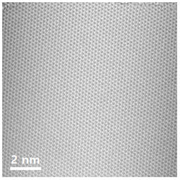
“This fold-free graphene film forms as a single crystal over the entire growth substrate because it shows a single orientation over LEED [large-area low-energy electron diffraction] patterns,” said fellow researcher Seong Won Kyung.
Graphene FETs patterned on the near-perfect graphene, in a variety of orientations with respect to the graphene, showed “remarkably uniform performance”, according to the Institute, with average room temperature electron and hole mobilities of 7×103cm2/V/s.
“Such remarkably uniform performance is possible because the fold-free graphene film is a single crystal with essentially no imperfections,” said Yunqing Li, a researcher from Ulsan National Institute of Science and Technology (UNIST), with which CMCM worked.
The process works across 1,000 to 1,030K and scales: with near-perfect graphene grown simultaneously on both sides of five 40 x 70mm CuNi foils in an IBS-built 150mm quartz furnace.
Electrochemical bubbling transfer lifted the graphene layers free, leaving the foils ready for re-use – after five growth cycles, the net loss of alloy from the foils was 100μg.
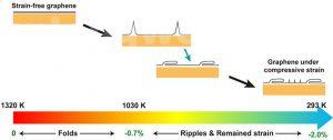

It transpired that ‘bunched step edge’ regions grow between single-crystal plateaus, and these regions de-laminate, allowing the material to climb off the substrate. “We discovered that step-bunching of a Cu-Ni(111) foil surface suddenly occurs at about 1,030K, and this surface reconstruction is the reason why the critical growth temperature of fold-free graphene is at ~1030 K or below,” said Ruoff.
The Institute expects the near-perfect graphene to be used, as it is or stacked with other 2D materials, in R&D towards electronic, photonic, mechanical and thermal devices. Stacking is particularly convenient as the graphene can be transferred from the CuNi foil to another substrate in less than a minute.
The work has been published in Nature.