“PWM rectifier is a new type of power converter developed by applying pulse width modulation technology. The basic principle is to make the input current of the rectifier close to a sine wave by controlling the on-off state of the power switch tube, and the current and voltage are in the same phase, thereby eliminating most of the current harmonics and making the power factor close to 1. This article uses TI’s TMS320F240DSP to implement digital control of the rectifier. This method has the following advantages over analog control.
“
Author: Liu Yanzhu
1 Introduction
PWM rectifier is a new type of power converter developed by applying pulse width modulation technology. The basic principle is to make the input current of the rectifier close to a sine wave by controlling the on-off state of the power switch tube, and the current and voltage are in the same phase, thereby eliminating most of the current harmonics and making the power factor close to 1. This article uses TI’s TMS320F240DSP to implement digital control of the rectifier. This method has the following advantages over analog control:
1) Flexible control In digital control systems, software algorithms are mainly used to implement control schemes, which are more flexible than analog control;
2) High reliability The microcomputer system uses fewer components and all signals are digitally processed, so the interference is small and the reliability is high;
3) Fault analysis is easy, signal detection will store the obtained information, and it has the ability to remember, so it is easy to realize fault diagnosis;
4) Simple parameter setting can make system debugging work very convenient.
Based on the above considerations, this article uses a digital control system with DSP as the core to control the rectifier.
2 Main features of TMS320F240
3 PWM rectifier main circuit and control scheme
The main circuit in this article adopts a single-phase full-bridge structure, as shown in Figure 1.


In the figure, uN


The specific control principle is briefly described as follows: The deviation of the output voltage sampling value (ud) and the given reference voltage (ud*) is sent to the PI regulator, and the obtained value is used as the amplitude of the reference current signal, multiplied by the same phase as the power supply voltage After the reference sine signal[sin(ωt)]it is used as the value of the reference current. The input current sampling value is obtained from the inductance circuit, and the current error signal is sent to the proportional regulator. The output value is added with the input voltage compensation signal[uT


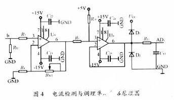
Current detection and conditioning unit circuit shown in Figure 4. After the output current signal of the current sensor is converted into a voltage signal by the measuring resistance RM, the gain of the amplifier formed by the operational amplifier U8 is determined by the value of RM, so that the output bipolar signal can fall within the range of ±5V. The operational amplifier U9 constitutes a level polarity conversion stage, which converts the bipolar signal into a unipolar signal in proportion. The unipolar 0~+5V signal is required for DSPA/D conversion, and the +5V power supply is supplied by the reference power supply composed of LM336. A simple low-pass filter composed of RC to filter out the sub-harmonics of the switching frequency of the AC input current, and the two diodes are clamping diodes.


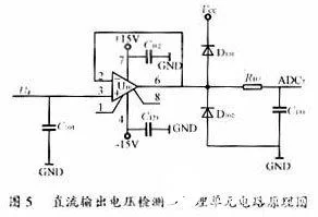
The DC output voltage detection and conditioning unit is a closed-loop front-end sensor for the DC side voltage. The purpose is to measure the DC side capacitor voltage. Since the capacitor voltage contains a certain ripple, it needs to introduce a filtering link. The circuit principle is shown in Figure 5.

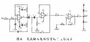
The AC input voltage signal is used as a synchronization signal. Since the voltage signal input from the power grid is often not a pure sine wave, it must be filtered to accurately detect the phase of the power grid input voltage. The filter includes a low-pass filter and a high-pass filter. part. The operational amplifier U11A and the peripheral resistance-capacitance network form a second-order low-pass filter. The low-pass filter can filter out high-order harmonics in the input signal of the power grid, so that the waveform is improved, but the phase is lagging, so a high-pass filter is introduced for compensation. U11B and its peripheral Resistor-capacitor network form a second-order high-pass filter. It can be seen from the circuit that the topological structure of the high-pass and low-pass filters are exactly the same, and the resistance and capacitance are symmetrically distributed. As long as the various parameters are selected appropriately, the leading phase of the high-pass filter can just offset the lagging phase of the low-pass filter. After filtering twice, not only the harmonics are filtered out, the waveform is close to sine, and there is no phase shift. After filtering, it passes through the zero-crossing hysteresis circuit to obtain a square wave signal that is completely synchronized with the input signal of the power grid. The circuit is shown in Figure 6.

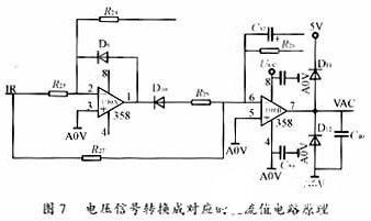
In addition, the detection of the input voltage value is not the instantaneous value of the voltage but the effective value, so the precision rectifier circuit shown in Fig. 7 is used to convert the filtered voltage signal into the corresponding DC value.

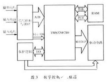
The CPU and its peripheral circuits mainly include clock circuits, reset circuits, and so on. In addition, for the convenience of debugging, this system has also expanded a 16-bit RAM chip as a program memory. The driving circuit plays a role in improving the driving capability and isolation of the pulse. The protection logic circuit ensures that when a fault occurs, the system can directly block the output pulse signal from the hardware.
5 Software design of the control system
The control system software in this article mainly includes the following parts:
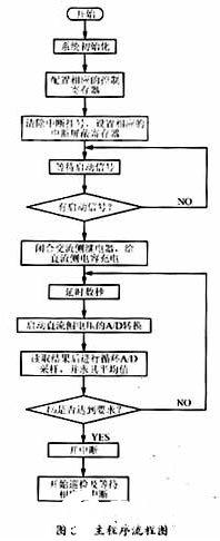
1) The main program mainly completes the initialization of the system and the loop detection of each input quantity in the system;
2) The current processing subroutine mainly completes the data processing of the current control loop in the control system;
3) The voltage processing subroutine mainly completes the data processing of the voltage control loop in the control system;
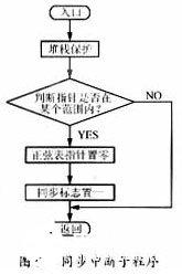
4) The synchronization interrupt subroutine takes the synchronization signal as the interrupt source and sets the synchronization flag to keep the software running rhythm of the entire control system consistent with the grid voltage;
5) Timer interrupt subroutine. This is the core part of the entire program, which generates the required PWM waves according to the results of each part of the operation.
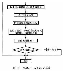
The software flow chart is shown in Figures 8, 9, and 10.


6 Experimental results
Using the above scheme, this article built a low-power experimental device in the laboratory, and the parameters of each part are as follows:
Input voltage AC 170V
Output voltage DC 300V
Output power 360W
The waveforms of each part are shown in Figures 11 and 12.


7 Conclusion
The PWM rectifier is a new type of power converter, which can make the input power factor close to 1. This paper adopts the current tracking control method, designs a digital control system with high-performance DSP chip TMS320F240 as the core, and conducts low-power experiments. Finally, the experiment proves that the control system has the advantages of flexible control, high precision, good dynamic response and little interference.
Author: Liu Yanzhu
1 Introduction
PWM rectifier is a new type of power converter developed by applying pulse width modulation technology. The basic principle is to make the input current of the rectifier close to a sine wave by controlling the on-off state of the power switch tube, and the current and voltage are in the same phase, thereby eliminating most of the current harmonics and making the power factor close to 1. This article uses TI’s TMS320F240DSP to implement digital control of the rectifier. This method has the following advantages over analog control:
1) Flexible control In digital control systems, software algorithms are mainly used to implement control schemes, which are more flexible than analog control;
2) High reliability The microcomputer system uses fewer components and all signals are digitally processed, so the interference is small and the reliability is high;
3) Fault analysis is easy, signal detection will store the obtained information, and it has the ability to remember, so it is easy to realize fault diagnosis;
4) Simple parameter setting can make system debugging work very convenient.
Based on the above considerations, this article uses a digital control system with DSP as the core to control the rectifier.
2 Main features of TMS320F240
3 PWM rectifier main circuit and control scheme
The main circuit in this article adopts a single-phase full-bridge structure, as shown in Figure 1.
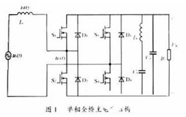
In the figure, uN
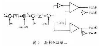
The specific control principle is briefly described as follows: The deviation of the output voltage sampling value (ud) and the given reference voltage (ud*) is sent to the PI regulator, and the obtained value is used as the amplitude of the reference current signal, multiplied by the same phase as the power supply voltage After the reference sine signal[sin(ωt)]it is used as the value of the reference current. The input current sampling value is obtained from the inductance circuit, and the current error signal is sent to the proportional regulator. The output value is added with the input voltage compensation signal[uT
Current detection and conditioning unit circuit shown in Figure 4. After the output current signal of the current sensor is converted into a voltage signal by the measuring resistance RM, the gain of the amplifier formed by the operational amplifier U8 is determined by the value of RM, so that the output bipolar signal can fall within the range of ±5V. The operational amplifier U9 constitutes a level polarity conversion stage, which converts the bipolar signal into a unipolar signal in proportion. The unipolar 0~+5V signal is required for DSPA/D conversion, and the +5V power supply is supplied by the reference power supply composed of LM336. A simple low-pass filter composed of RC to filter out the sub-harmonics of the switching frequency of the AC input current, and the two diodes are clamping diodes.
The DC output voltage detection and conditioning unit is a closed-loop front-end sensor for the DC side voltage. The purpose is to measure the DC side capacitor voltage. Since the capacitor voltage contains a certain ripple, it needs to introduce a filtering link. The circuit principle is shown in Figure 5.

The AC input voltage signal is used as a synchronization signal. Since the voltage signal input from the power grid is often not a pure sine wave, it must be filtered to accurately detect the phase of the power grid input voltage. The filter includes a low-pass filter and a high-pass filter. part. The operational amplifier U11A and the peripheral resistance-capacitance network form a second-order low-pass filter. The low-pass filter can filter out high-order harmonics in the input signal of the power grid, so that the waveform is improved, but the phase is lagging, so a high-pass filter is introduced for compensation. U11B and its peripheral resistor-capacitor network form a second-order high-pass filter. It can be seen from the circuit that the topological structure of the high-pass and low-pass filters are exactly the same, and the resistance and capacitance are symmetrically distributed. As long as the various parameters are selected appropriately, the leading phase of the high-pass filter can just offset the lagging phase of the low-pass filter. After filtering twice, not only the harmonics are filtered out, the waveform is close to sine, and there is no phase shift. After filtering, it passes through the zero-crossing hysteresis circuit to obtain a square wave signal that is completely synchronized with the input signal of the power grid. The circuit is shown in Figure 6.

In addition, the detection of the input voltage value is not the instantaneous value of the voltage but the effective value, so the precision rectifier circuit shown in Fig. 7 is used to convert the filtered voltage signal into the corresponding DC value.

The CPU and its peripheral circuits mainly include clock circuits, reset circuits, and so on. In addition, for the convenience of debugging, this system has also expanded a 16-bit RAM chip as a program memory. The driving circuit plays a role in improving the driving capability and isolation of the pulse. The protection logic circuit ensures that when a fault occurs, the system can directly block the output pulse signal from the hardware.
5 Software design of the control system
The control system software in this article mainly includes the following parts:
1) The main program mainly completes the initialization of the system and the loop detection of each input quantity in the system;
2) The current processing subroutine mainly completes the data processing of the current control loop in the control system;
3) The voltage processing subroutine mainly completes the data processing of the voltage control loop in the control system;
4) The synchronization interrupt subroutine takes the synchronization signal as the interrupt source and sets the synchronization flag to keep the software operation rhythm of the entire control system consistent with the grid voltage;
5) Timer interrupt subroutine. This is the core part of the entire program, which generates the required PWM waves according to the results of each part of the operation.
The software flow chart is shown in Figures 8, 9, and 10.

6 Experimental results
Using the above scheme, this article built a low-power experimental device in the laboratory, and the parameters of each part are as follows:
Input voltage AC 170V
Output voltage DC 300V
Output power 360W
The waveforms of each part are shown in Figures 11 and 12.

7 Conclusion
The PWM rectifier is a new type of power converter, which can make the input power factor close to 1. This paper adopts the current tracking control method, designs a digital control system with high-performance DSP chip TMS320F240 as the core, and conducts low-power experiments. Finally, the experiment proves that the control system has the advantages of flexible control, high precision, good dynamic response and little interference.
The Links: R0878LS20K LMG6381QHGE