An IGBT module consists of multiple interconnected IGBT chips, with electrical connections established through aluminum wires. In a standard IGBT package, each IGBT chip is usually combined with a freewheeling diode and encapsulated in a plastic casing filled with a significant amount of silicone gel. The IGBT chip stack structure is shown in Figure 1-1.

From top to bottom, it consists of the chip, DBC (Directed Bonding Copper), and a metal heat sink (often made of copper). The DBC is composed of three layers: two metal layers on the top and bottom, with an intermediate insulating ceramic layer. Compared to ceramic substrates, DBC offers better performance advantages, such as lighter weight, improved thermal conductivity, and enhanced reliability.
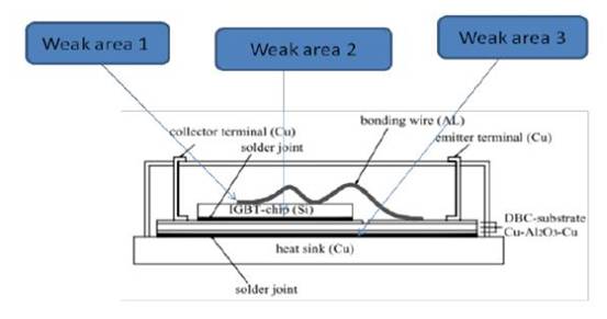
- Failure Mechanisms in IGBT Packaging
The reliability of power devices refers to their ability to function under specified conditions, usually expressed in terms of their operational lifespan. As power Semiconductor devices are primarily used for current switching, they generate significant power losses. Therefore, thermal management is crucial in the design of power electronic systems. In the operation of power electronic devices, the primary concern is thermal issues, including steady-state temperature, temperature cycling, temperature gradients, and the compatibility of packaging materials with operating temperatures.
Due to the adoption of stacked packaging technology in IGBTs, which improves packaging density and reduces interconnection lengths between chips, the reliability of IGBTs has been questioned. It is easy to imagine that failures in IGBT module packaging primarily occur at the bonding points of wire connections, chip attachments, substrate attachments, and substrates.
In typical power cycling or temperature cycling, the chip, solder layers, substrate, baseplate, and package housing all experience varying degrees of temperature and temperature gradients. The coefficient of thermal expansion (CTE) is an important material property that measures the dimensional change per degree temperature increase within a specific temperature range. Figure 1-2 shows the CTE of commonly used materials in IGBT stack structures. Due to the different CTEs of these materials, the thermal strains between different materials vary during temperature changes, leading to fatigue and failure at the interfaces. Therefore, the thermal behavior of the device is closely related to the module’s packaging structure. Investigations have shown that for every 10°C increase in operating temperature, the failure rate due to temperature-related effects doubles.


- 3 Detachment of Aluminum Bonding Wires
The diameter of aluminum bonding wires inside IGBTs typically ranges from 300 to 500 μm, and their chemical composition may vary depending on the manufacturer. However, in almost all cases, a small amount of alloy, such as silicon-magnesium or silicon-nickel alloy, is added to pure aluminum to significantly increase its hardness and corrosion resistance. Due to the disproportional relationship with length and slight dependence on substrate temperature, the current-carrying capacity of bonding wires decreases. Direct current flow is limited by the melting caused by the wire’s own Ohmic heating effect. Since aluminum bonding wires are directly attached to chips or pressure buffers, they experience significant temperature variations. Moreover, IGBT modules consist of materials with different coefficients of thermal expansion, leading to pronounced thermal fatigue during operation. This fatigue becomes more evident over time as the wire’s Ohmic effect becomes more pronounced, eventually resulting in cracks at the base of the bonding wire.
- 4 Reconstruction of Aluminum Wires
In thermal cycling tests, the mismatch in coefficients of thermal expansion causes periodic compression and elongation on the bonding surface, which exceeds the material’s own range of expansion and contraction. Under such conditions, the pressure is released through mechanisms like diffusion creep, grain slippage, and dislocation. The reshaping of aluminum leads to a decrease in the effective contact area, leading to an increase in contact resistance. This also explains why Vce linearly increases during periodic testing.
- 5 Solder Fatigue and Solder Voids
Cracks in the solder layer between the chip and substrate, caused by the different coefficients of thermal expansion, increase the contact resistance of the wires. The increased resistance enhances the Ohmic effect, leading to temperature positive feedback and exacerbating the cracks, eventually resulting in device failure. Voids within the solder layer affect the thermal cycling of the device, reducing its heat dissipation performance, which further accelerates the temperature rise and module damage. Additionally, there is hysteresis between stress and strain, and during continuous temperature cycling, the material’s shape undergoes real-time changes, increasing the thermal fatigue of the solder. Furthermore, voids introduced by process issues in the solder affect the thermal cycling during operation, causing localized high temperatures, which is another significant cause of module failure.
- 6 Wafer and Ceramic Cracks
In the seven-layer structure of IGBTs, the mismatch in coefficients of thermal expansion imposes significant mechanical stress on each layer. Under temperature differentials, the deformation of different layers varies, and different parts of the same layer also experience different degrees of deformation due to temperature distribution differences. This inevitably leads to localized excessive stress, resulting in material cracking.