EMI problems are often the last major bottleneck at the end of product development. Modeling and first measurements help to reduce the risk, but especially when a compact design is required, there is little space for last-minute changes. As time scales slip, the prices of the components used increase in proportion to the desperation and pressure to get the unit to market.
The Problems of EMI
I have rarely seen EMI filters being cost optimised once a solution has been found. Time, engineering budgets and risk do not allow it; making it even more important to have a good and cost effective EMI solution from the start. Recently I was helping to debug a 3kW single phase unit with a standard boost PFC. The Transistor a standard 650V T0-247 super junction MOSFET was injecting lots of common-mode noise into the chassis. Eliminating the source of the noise by replacing the mosfet with a source tabbed, Nexperia GAN063-650W, was a simple and cost effective solution. This article shows measurements and diagnostic methods.
LISN
EMI measurements are conducted using a LISN at the power supply input. The LISN provides a defined source impedance for the measurements as well as removing low-frequency signals.

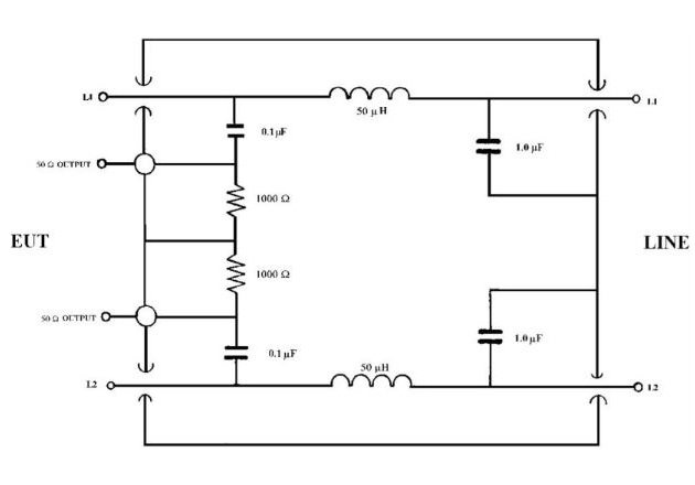
Figure 1: Standard LISN
Figure 1 shows the standard LISN. The 50Ω termination in the receiver with the 100nF cap, give an LF cut-off frequency of 30kHz; which effectively removes mains ripple from the measurement so the small level disturbances can be seen by the receiver. To look at the HF disturbance with a scope, it is necessary to remove the dominant mains. A 50Ω system as used in the LISN would change the system and significantly distort the measurements, so a high impedance filter (1nF cap with 10k to GND) was used. The filter removes the low frequency components. Only the HF noise is visible without significantly loading the circuit. The scope maths channel was used to calculate the differential part of the noise. (ch1-ch2) and to get a feeling in realtime how effective the filter is.
Measurements
Using the HF filter, the noise can be seen at various nodes around the PFC schematic (Figure 2). The overlaid green and yellow traces show the voltage to ground, and the light blue trace is the differential voltage. Note the scaling is 2V/div and 1V div for the maths channel.
Looking at the various plots; (5) the output, after the Inductor has almost no common mode noise (blue). At the mosfet (4), the common-mode noise can be clearly seen to be synchronised with the switching of the mosfet. Plot 3 shows the noise that the filter should attenuate, common-mode noise is dominant, but also significant differential noise. Plot 2 shows the noise after one filter stage. The scaling is the same as plot 3, switching frequency common-mode noise has been reduced 14dB from ~1V to ~200mV; we could expect more from a filter stage.
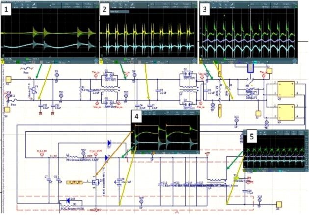
Figure 2: HF noise around the schematic
The plots clearly show noise is produced by the mosfet (no great surprise!), but more surprisingly most of the high frequency noise is common-mode (plots1-3). Removing the drain from the grounded heatsink confirmed that the capacitance of the mosfet case, switching 400V in 20nS, generates most of the common mode noise.
Current injected into the heatsink The mosfet tab has an area of about 245mm². It is mounted on a 100μm isolator which creates a capacitance of around 120pF to the heatsink. At 20V/nS, the current injected into the heatsink is 400mA. The return part for this current is first the local Y caps. Ignoring
inductance; the voltage over the Y Capacitors can be calculated as a voltage divider; tab capacitance with 120pF and 400V divided by the Y Capacitors (2x4n7), resulting in 5V (134dBμV) over the Ycap (close to the measured value). To meet a 65dBμV EMC limit; a filter with about 70dB attenuation would be required. As the Y capacitance value is limited due to earth leakage currents, only the inductance can be increased. A 2-stage filter with 65dB at 200kHz could have 10mF and 10nF Ycaps, which is large and expensive.
A thicker isolator such as 2mm alumina can reduce the capacitance by a factor of 10, but in this application, heatsink paste would be needed, and thermal resistance would be significantly degraded. The first rule of good EMI practice is to eliminate noise generators at source when possible; here it is easy, a Transistor with the cooling tab connected to source would eliminate the switched voltage charge injection into the heatsink. TO-247 packed GaN transistors with source connected cooling are available from multiple vendors with source tabs, Nexperia kindly sampled the GaN-063-650W.
Modifications for the GaN Transistor
The first thing to note is the GaN has a different pinout to a standard T0-247. The standard MOSFET has, the drain in the middle; the GaN has the source as the centre pin. To replace the MOSFET with the GaN Transistor; the GaN legs had to be bent, with the drain and source being effectively swapped. PTFE sleeving was used to guarantee isolation. Reforming the leads meant that the source on the GaN is longer than usual and has more inductance; which could create problems with switching and possible oscillation at high currents. This isn’t ideal, but does permit a quick first look without a redesign of the board.
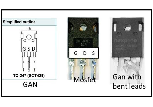
Figure 3: Reforming Gan legs
The GaN gate charge with15nC is about a tenth of a similar MOSFET, so the gate Resistor was increased to 18Ω it also meant that the extra driver stage could be removed and the Transistor could be driven directly from the PFC controller.
Measurements
Figure 4 shows comparable drain-source switching waveforms. The first surprise was clean switching waveforms, despite the bent leads. Turn-off Switching speeds (dV/dt) are similar, but the GaN does not have the initial slow rise time at the beginning of turn-off. The short delay between the gate going low and switching is a benefit of the much much smaller output capacitance at Vds<50V. The GaN turnon is somewhat faster, with 40V/nS is it about twice as fast as the MOSFET, ringing at turn-off is similar. There is more ringing at turn-on which not too surprising considering how the transistor is mounted with extended reformed leads with a very long source lead.
EMI plots in figure 5 show clearly, the benefit of the source connected tab. The whole spectrum looks cleaner, with about 10dB lower emissions at 170kHz. Tests showed the 170kHz emissions could be further reduced by adding a larger x capacitor, whereas with the MOSFET larger Ycaps and Xcaps would be needed. The MOSFET has a rise time of 20nS, compared to the GaN 10nS so that the GaN noise spectrum would have the double cut off frequency, but more important is the virtual elimination of the capacitance of the switched drain to the heatsink. With the injected currents in the chassis eliminated by using the GaN; we expected the chassis to be quiet. Further investigation revealed the inductance of the SiC diode cathode lead, was now the primary noise injector into the chassis. The switched current in the cathode lead inductance, induce a voltage on the tab. This voltage is capacitively coupled to the heatsink and injects current into the chassis. As there is no large voltage here, a small snubber between the diode lead and elco removed most of the noise with minimal cost and power loss. Typical EMC, remove one source of noise only to then discover more.
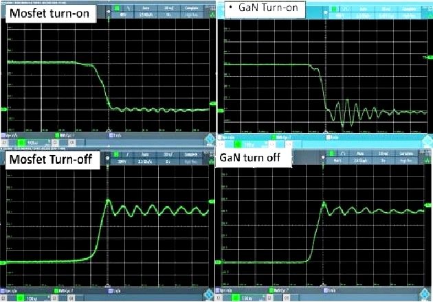
Figure 4: Switching Waveform Comparison
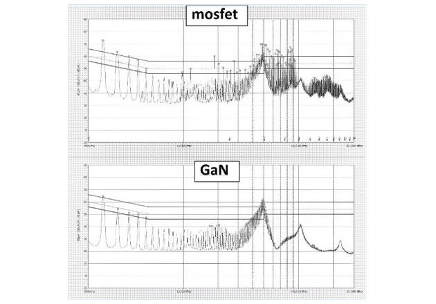
Figure 5: EMI Measurement Mosfet and GaN
Conclusion
Using the source tabbed transistor eliminated a significant source of EMI at its origin. I was surprised by how well the GaN performed despite having the long bent leads. The pinout with the source centre pin TO-247 will allow a much better layout than the current drain tabbed transistor, with probably more EMI improvements and lower losses.