“ESD protection design is becoming more and more difficult with the improvement of CMOS process level. ESD protection is not only an ESD protection design problem of input pins or output pins, but a problem of ESD protection of the whole chip. Each I/O circuit in the chip needs to establish a corresponding ESD protection circuit. In addition, considering the entire chip, the use of a whole-chip protection structure is a good choice, and it can also save I/OPAD. The area of the ESD component.
“
1 Introduction
Electrostatic discharge (ESD-ElectroStatic Discharge) can bring destructive consequences to Electronic devices and is one of the main reasons for the failure of integrated circuits. With the continuous development of integrated circuit technology, the size of CMOS circuits continues to shrink, the thickness of the gate oxide of the tube is getting thinner and thinner, the area of the chip is getting larger and larger, the current and voltage that the MOS tube can withstand is getting smaller and smaller, and the periphery The environment of use has not changed, so it is necessary to further optimize the anti-ESD performance of the circuit.
How to make the effective area of the whole chip as small as possible, high ESD resistance and no need to add additional process steps has become the main consideration for IC designers.
2. ESD protection principle
The design purpose of the ESD protection circuit is to prevent the working circuit from becoming damaged due to ESD, and to ensure that the ESD that occurs between any two chip pins has a low resistance bypass to introduce ESD current into the power line. This low-impedance bypass must not only absorb the current generated by ESD, but also clamp the voltage of the working circuit to prevent the working circuit from being damaged due to voltage overload. When the circuit is working normally, the antistatic structure does not work, which makes the ESD protection circuit also need to have good stability, can respond quickly when ESD occurs, while protecting the circuit, the antistatic structure itself is not damaged. The negative effects of the antistatic structure (such as input delay) must be within an acceptable range and prevent the antistatic structure from latching up.
3. Design of CMOS circuit ESD protection structure
Most of the ESD current comes from outside the circuit, so the ESD protection circuit is generally designed next to the PAD or inside the I/O circuit. A typical I/O circuit consists of two parts: output driver and input receiver. ESD is introduced into the chip through the PAD, so all the devices directly connected to the PAD in the I/O need to establish a parallel ESD low-impedance bypass to introduce the ESD current into the voltage line, and then distribute the voltage line to the various pins of the chip. Reduce the impact of ESD. Specific to the I/O circuit, it is the output driver and input receiver connected to the PAD. It must be ensured that when ESD occurs, a low resistance path parallel to the protection circuit is formed, bypassing the ESD current, and can effectively clamp the protection circuit immediately Voltage. When these two parts work normally, it does not affect the normal operation of the circuit. Commonly used ESD protection devices include resistors, diodes, bipolar transistors, MOS tubes, thyristors and so on. Because the MOS tube has good compatibility with the CMOS process, the MOS tube is often used to construct the protection circuit.
The NMOS Transistor under the CMOS process has a lateral parasitic npn (source-p-type substrate-drain) Transistor, which can absorb a large amount of current when it is turned on. Using this phenomenon, a protection circuit with a higher ESD withstand voltage can be designed in a smaller area. A typical device structure is the gate grounded NMOS (GGNMOS, GateGroundedNMOS).
Under normal working conditions, the NMOS lateral transistor will not turn on. When ESD occurs, an avalanche occurs in the drain and the depletion region of the substrate, and electron-hole pairs are also generated at the same time. A part of the generated holes is absorbed by the source, and the rest flows through the substrate. Due to the existence of the substrate resistance Rsub, the substrate voltage is increased. When the PN junction between the substrate and the source is positively biased, electrons are emitted from the source into the substrate. Under the action of the electric field between the source and drain, these electrons are accelerated, resulting in collision ionization of electrons and holes, forming more electron-hole pairs, increasing the current flowing through the npn transistor, and eventually causing the NMOS transistor to undergo two cycles. Second breakdown, the breakdown at this time is no longer reversible, and it will eventually cause the NMOS tube to be damaged.
In order to further reduce the voltage at both ends of the NMOS on the output drive during ESD, a Resistor can be added between the ESD protection device and the GGNMOS. This resistance cannot affect the working signal, so it cannot be too large. Polysilicon (poly) resistors are usually used when drawing layouts.
Only yi-level ESD protection is used, and the tube inside the circuit may still be broken down when the ESD current is large. GGNMOS is turned on. Due to the large ESD current, the resistance on the substrate and the metal connection cannot be ignored. At this time, GGNMOS cannot clamp the voltage input to the receiving terminal gate, because the voltage of the silicon oxide layer of the receiving terminal gate is input. What reaches the breakdown voltage is the IR voltage drop between the GGNMOS and the substrate of the input receiving end. In order to avoid this situation, a small size GGNMOS can be added near the input receiving terminal for secondary ESD protection, and it can be used to clamp the gate voltage of the input receiving terminal, as shown in the figure below.
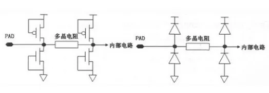
Common ESD protection structure and equivalent circuit

When drawing the layout, care must be taken to place the secondary ESD protection circuit close to the input receiving terminal to reduce the resistance of the substrate and its wiring between the input receiving terminal and the secondary ESD protection circuit. In order to draw a large-size NMOS tube in a smaller area, it is often drawn as a finger in the layout, and the I/O ESD design rules should be strictly followed when drawing the layout.
If the PAD is only used as an output, the protection resistor and the NMOS with a short end to the ground are not needed. The large-size PMOS and NMOS devices of the output stage can themselves be used as ESD protection devices. Generally, the output stage has a double protection ring, so that it can be used. Prevent latch-up.
When designing a full-chip ESD structure, pay attention to the following principles:
(1) The peripheral VDD and VSS traces should be as wide as possible to reduce the resistance of the traces;
(2) Design a voltage clamping structure between VDD-VSS and provide a direct low-impedance current discharge channel for VDD-VSS when ESD occurs. For circuits with larger areas, it is good to place one such structure around the chip. If possible, placing multiple VDD and VSS PADs on the periphery of the chip can also enhance the ESD resistance of the overall circuit;
(3) The power and ground traces of the peripheral protection structure should be separated from the internal traces as much as possible, and the peripheral ESD protection structure should be designed uniformly as far as possible to avoid ESD weak links in the layout design;
(4) The design of ESD protection structure should balance the influence of circuit ESD performance, chip area, and protection structure on circuit characteristics, such as input signal integrity, circuit speed, output drive capability, etc., and also need to consider the capacity of the process. Poor, so that the circuit design is very optimized;
(5) In some circuits actually designed, sometimes there is no direct VDD-VSS voltage clamping protection structure. At this time, the voltage clamping and ESD current discharge between VDD-VSS mainly use the well and the whole circuit of the whole chip. The contact space of the substrate. Therefore, in the peripheral circuit, the contact between the well and the substrate should be increased as much as possible, and the spacing of the NPs should be consistent. If there is space, it is better to add a VDD-VSS voltage clamp protection structure beside and around the PAD of VDD and VSS, which not only enhances the ESD resistance in VDD-VSS mode, but also enhances the I/O mode in I/O mode. The anti-ESD ability.
Generally, as long as the above-mentioned general principles are adopted, considering the compromise with the chip area, the anti-ESD voltage of a general sub-micron CMOS circuit can reach more than 2500V, which can already meet the anti-ESD requirements of commercial circuit designs.
For the design of deep sub-micron ultra-large-scale CMOSIC, conventional ESD protection is not used
1 Introduction
Electrostatic discharge (ESD-ElectroStatic Discharge) can bring destructive consequences to electronic devices and is one of the main reasons for the failure of integrated circuits. With the continuous development of integrated circuit technology, the size of CMOS circuits continues to shrink, the thickness of the gate oxide of the tube is getting thinner and thinner, the area of the chip is getting larger and larger, the current and voltage that the MOS tube can withstand is getting smaller and smaller, and the periphery The environment of use has not changed, so it is necessary to further optimize the anti-ESD performance of the circuit.
How to make the effective area of the whole chip as small as possible, high ESD resistance and no need to add additional process steps have become the main considerations of IC designers.
2. ESD protection principle
The design purpose of the ESD protection circuit is to prevent the working circuit from becoming damaged due to ESD, and to ensure that the ESD that occurs between any two chip pins has a low resistance bypass to introduce ESD current into the power line. This low-impedance bypass must not only absorb the current generated by ESD, but also clamp the voltage of the working circuit to prevent the working circuit from being damaged due to voltage overload. When the circuit is working normally, the antistatic structure does not work, which makes the ESD protection circuit also need to have good stability, can respond quickly when ESD occurs, while protecting the circuit, the antistatic structure itself is not damaged. The negative effects of the antistatic structure (such as input delay) must be within an acceptable range and prevent the antistatic structure from latching up.
3. Design of CMOS circuit ESD protection structure
Most of the ESD current comes from outside the circuit, so the ESD protection circuit is generally designed next to the PAD or inside the I/O circuit. A typical I/O circuit consists of two parts: output driver and input receiver. ESD is introduced into the chip through the PAD, so all the devices directly connected to the PAD in the I/O need to establish a parallel ESD low-impedance bypass to introduce the ESD current into the voltage line, and then distribute the voltage line to the various pins of the chip. Reduce the impact of ESD. Specific to the I/O circuit, it is the output driver and input receiver connected to the PAD. It must be ensured that when ESD occurs, a low-impedance path parallel to the protection circuit is formed, bypassing the ESD current, and can effectively clamp the protection circuit immediately Voltage. When these two parts work normally, it does not affect the normal operation of the circuit. Commonly used ESD protection devices include resistors, diodes, bipolar transistors, MOS tubes, thyristors and so on. Because the MOS tube has good compatibility with the CMOS process, the MOS tube is often used to construct the protection circuit.
The NMOS transistor under the CMOS process has a lateral parasitic npn (source-p-type substrate-drain) transistor, which can absorb a large amount of current when it is turned on. This phenomenon can be used to design a higher ESD withstand voltage protection circuit in a smaller area. A typical device structure is the gate grounded NMOS (GGNMOS, GateGroundedNMOS).
Under normal working conditions, the NMOS lateral transistor will not turn on. When ESD occurs, an avalanche occurs in the drain and the depletion region of the substrate, and electron-hole pairs are also generated at the same time. A part of the generated holes is absorbed by the source, and the rest flows through the substrate. Due to the existence of the substrate resistance Rsub, the substrate voltage is increased. When the PN junction between the substrate and the source is positively biased, electrons are emitted from the source into the substrate. Under the action of the electric field between the source and drain, these electrons are accelerated, resulting in collision ionization of electrons and holes, forming more electron-hole pairs, increasing the current flowing through the npn transistor, and eventually causing the NMOS transistor to undergo two cycles. Second breakdown, the breakdown at this time is no longer reversible, and it will eventually cause the NMOS tube to be damaged.
In order to further reduce the voltage at both ends of the NMOS on the output drive during ESD, a resistor can be added between the ESD protection device and the GGNMOS. This resistance cannot affect the working signal, so it cannot be too large. Polysilicon (poly) resistors are usually used when drawing layouts.
Only yi-level ESD protection is used, and the tube inside the circuit may still be broken down when the ESD current is large. GGNMOS is turned on. Due to the large ESD current, the resistance on the substrate and the metal connection cannot be ignored. At this time, GGNMOS cannot clamp the voltage input to the receiving terminal gate, because the voltage of the silicon oxide layer of the receiving terminal gate is input. What reaches the breakdown voltage is the IR voltage drop between the GGNMOS and the substrate of the input receiving end. To avoid this situation, a small size GGNMOS can be added near the input receiving end for secondary ESD protection, and it can be used to clamp the gate voltage of the input receiving end, as shown in the figure below.

Common ESD protection structure and equivalent circuit
When drawing the layout, care must be taken to place the secondary ESD protection circuit close to the input receiving terminal to reduce the resistance of the substrate and its wiring between the input receiving terminal and the secondary ESD protection circuit. In order to draw a large-size NMOS tube in a small area, it is often drawn as a finger in the layout. When drawing the layout, the design rules of I/O ESD should be strictly followed.
If the PAD is only used as an output, the protection resistor and the NMOS with a short end to the ground are not needed. The large-size PMOS and NMOS devices of the output stage can themselves be used as ESD protection devices. Generally, the output stage has a double protection ring, so that it can be used. Prevent latch-up.
When designing a full-chip ESD structure, pay attention to the following principles:
(1) The peripheral VDD and VSS traces should be as wide as possible to reduce the resistance of the traces;
(2) Design a voltage clamping structure between VDD-VSS and provide a direct low-impedance current discharge channel for VDD-VSS when ESD occurs. For circuits with larger areas, it is good to place one such structure around the chip. If possible, placing multiple VDD and VSS PADs on the periphery of the chip can also enhance the ESD resistance of the overall circuit;
(3) The power and ground traces of the peripheral protection structure should be separated from the internal traces as much as possible, and the peripheral ESD protection structure should be designed uniformly as far as possible to avoid ESD weak links in the layout design;
(4) The design of ESD protection structure should balance the influence of circuit ESD performance, chip area, and protection structure on circuit characteristics, such as input signal integrity, circuit speed, output drive capability, etc., and also need to consider the capacity of the process. Poor, so that the circuit design is very optimized;
(5) In some circuits actually designed, sometimes there is no direct VDD-VSS voltage clamping protection structure. At this time, the voltage clamping and ESD current discharge between VDD-VSS mainly use the well and the whole circuit of the whole chip. The contact space of the substrate. Therefore, in the peripheral circuit, the contact between the well and the substrate should be increased as much as possible, and the spacing of the NPs should be consistent. If there is space, it is better to add a VDD-VSS voltage clamp protection structure beside and around the PAD of VDD and VSS, which not only enhances the ESD resistance in VDD-VSS mode, but also enhances the I/O mode in I/O mode. The anti-ESD ability.
Generally, as long as the above-mentioned general principles are adopted, considering the compromise with the chip area, the anti-ESD voltage of a general sub-micron CMOS circuit can reach more than 2500V, which can already meet the anti-ESD requirements of commercial circuit designs.
For the design of deep sub-micron ultra-large-scale CMOSIC, conventional ESD protection is not used
The Links: NL6448BC33-74 PM15CSJ060