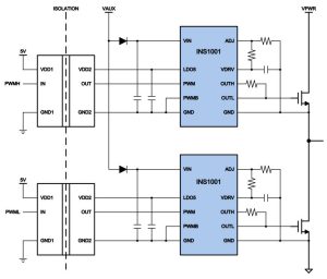

The single-channel INS1001DE is intended to supply fast powerful voltage-regulated waveforms to the gates, which are extremely sensitive to over-voltage stress.
Its output pulse amplitude is set by a low-drop-out regulator using two resistors, to, for example 6V which is commonly specified for enhancement-mode GaN hemts (diagram below right).


A separate internal LDO provides 5V for the internal logic, from an external supply of 6 to 20V.
No isolation is included, but 5V is provided out of the IC to supply an external front-end digital isolator.
The output stage has a 1.3Ω pull-up and 500mΩ pull-down, with separate pads to allow separate pull-ip and pull-down resistors to set turn on turn-off times.
Into a 1nF gate, typical rise-time down to 10ns are available, and fall-times down to 3ns. Propagation delay through the device is 35ns (50ns max).


Packaging is a 3 x 3mm DFN3x3-10L with thermal pad.
“The INS1001DE is perfectly matched to optimize the performance of e-mode GaN HEMTs, and particularly innoscience’s e-mode InnoGaN,” said the company’s v-p of IC design Min Chen.