The impressive qualities of wide-bandgap (WBG) semiconductors such as gallium nitride (GaN) and silicon carbide (SiC) have made them appealing to several markets, including electric vehicles, PV inverters, fast chargers, and telecommunications. GaN and SiC are focused on the energy required to shift electrons in these materials from the valence band to the conduction band. This energy, or bandgap, is 1.1 eV for silicon (Si), about 3.2 eV for SiC, and 3.4 eV for GaN. Those properties lead to a higher applicable breakdown voltage, which can reach up to 1,700 V in some applications.
5G is the latest-generation network that is poised to power the internet of things. Networks running 5G will be up to 20× faster than the existing 4G network, enabling video-download speeds up to 10× faster. High-performance power semiconductors such as GaN and SiC are playing a key role in 5G radio-frequency (RF) solutions, wireless power transfer (WPT), and base-station power supplies.
To meet power requirements in these applications, OEMs are turning to GaN in particular. A GaN-based power system can offer a good option to support the stringent demands of data transmission and energy-efficiency requirements.
5G base stations need to transmit signals in low, medium, and mmWave bands. As frequencies increase, so does the power required to transmit over useful distances. Because of its high-frequency characteristics, GaN offers advantages over other processes for use in 5G base-station power amplifiers (PAs).

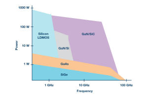
Figure 1: Comparing power and frequency of different materials in the microwave range, which includes mmWave (Source: Analog Devices Inc.)
The stringent requirements for 5G involve macro-scale densification, with multiple base stations and power densification at the device level. Yole Développement predicts that GaN will significantly penetrate two markets with a compound annual growth rate of 20% over the next decades, namely for defense and wireless telecommunications. GaN will play a key role in high-performance wireless solutions with its power-efficiency levels and high-frequency performance.
Gallium nitride
Compared with Si and gallium arsenide (GaAs) Semiconductor materials, GaN and SiC are both broadband compound semiconductor wafers, which have the characteristics of a high breakdown electric field strength, high saturated electron drift velocity, high thermal conductivity, and low dielectric constant. The low-loss and high-switching–frequency characteristics are suitable for the manufacture of high-frequency, high-power, small-volume (size), and high-density electronic devices.
The GaN material for 5G semiconductor manufacturers is oriented toward the field of microwave, high-frequency, and low-power (less than 1,000 V) devices and lasers. Compared with Si laterally diffused metal-oxide semiconductor (LDMOS) technology and GaAs solutions, GaN devices can provide more power and bandwidth.
GaN power semiconductors will make a leap in power density and packaging every year and can be better-adapted to massive MIMO technology. GaN high-electron–mobility Transistor (HEMT) semiconductor epitaxy has become an important technology for PAs used in 5G macro base stations.
The market for RF power devices for base stations was worth $1.1 billion in 2014, when GaN accounted for an 11% share and LDMOS’s share was 88%, according to Yole Développement. This estimate increased to a 25% share by 2017 and is trending upward (Figure 2). Yole forecasts that the total GaN RF device market will exceed $2.4 billion by 2026, dominated by 5G telecom infrastructure and defense applications, representing 41% and 49% of the market, respectively.

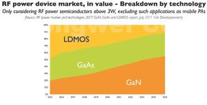
Figure 2: GaN is forecast to dominate the RF power device market by 2025. (Source: Yole Développement)
GaN-on-SiC solutions are a prime candidate for 5G telecom, as they offer high efficiency in a Doherty configuration at higher frequencies over a wider bandwidth than Si LDMOS transistors. GaN Transistor technology can also be quite robust, operating with severe load mismatches at high power with minimal performance degradation.
The mmWave spectrum is critical to the realization of 5G. Small cells can be placed close together in urban environments for line-of-sight links, mitigating the lossy propagation properties of high-frequency signals.
5G and power management
In semiconductor manufacturing, GaN is usually grown at high temperature (about 1,100°C) by metal organic chemical vapor deposition or molecular beam epitaxy techniques on a SiC substrate for RF applications, or silicon for power electronic applications.
The GaN-on-Si combination does not perform well, as it exhibits higher RF losses, but it proves to be cheaper. GaN-on-SiC, on the other hand, stands out in RF applications for several reasons: The GaN material offers much higher voltages than other semiconductor devices, as mentioned above, and it also guarantees high saturation rates. When GaN is combined with a large charge capacity, this translates into much higher current density for devices. The SiC substrate has a relatively high thermal conductivity (~120 W/mK), so heat can be more easily removed from the transistor to the heat sink.
The quality of the 5G coverage depends on many elements, including the surrounding environment. The 5G signal can be interrupted by walls, water towers, and other barriers to RF propagation. The maturation of 5G technology supported by WBG semiconductors, IoT, and wireless charging will work together to create more technological innovation for the 5G infrastructure.
Magnetic-resonance–based WPT technologies such as AirFuel’s technology have emerged in recent years on the strength of their high operating frequency (6.78 MHz) and ability to offer location flexibility, extended range, and multi-device charging capabilities. The wireless technology is well-known, but the design of transmitters, their location, maximizing efficiency, and validating the behavior of the entire system represent big challenges that require the use of complex engineering solutions.
The advent of 5G networks will see the use of mmWave frequencies with large bandwidth. In fixed wireless access (FWA) applications, the external network unit needs power from the internal power line and adapters. Instead of wired solutions, a WPT system can be used for power transfer for the external network unit and also be used for 5G micro base stations and IoT devices such as IP cameras and optical network terminals (fiber-to-home).
The conventional WPT system consists of a constant-current RF source with a PA and coils that act as a transmitter (Tx) and receiver (Rx) with specific characteristics. On the receiver side, a full-bridge rectifier transforms the coupled RF power into a DC signal. A solution for PAs is provided by GaN technology devices, which can offer more than 80% efficiency end to end, on par with wired systems, over a very wide impedance range.
Coupling coils must be optimized by offering a high coupling factor (Q). The Q of the transmitter coil should be large enough to achieve a high mutual coupling factor to transfer more power to the other side of the wall in FWA applications. Based on calculations from GaN Systems, a typical coil size of 200 × 200 mm is large enough to transfer power at a distance of 250 mm. GaN Systems’ engineers used a Class EF2 amplifier topology and a combination of T-type plus Pi-type impedance matching.


Figure 3: GaN Systems’ WPT system for 5G FWA outdoor-unit charging applications (Source: GaN Systems)
New developments
Chipmakers are starting to focus more of their GaN power semiconductor technology development for the 5G market. One example is Mitsubishi Electric Corp.’s GaN PA module, measuring 6 × 10 mm, for 5G base stations. This device requires a minimum number of SMD components, including capacitors and inductors, in the coupling circuit to control the high-quality signal output. The integrated GaN transistors help to increase the efficiency of the power amplifier.
The use of SMD devices for the coupling circuit can reduce the size of the form factor but can also reduce the energy efficiency, as these devices tend to have high power loss. Mitsubishi Electric’s new technology, however, creates a coupling circuit using a reduced number of SMDs while offering higher power efficiency. The SMDs also offer the same electrical characteristics as metal foil transmission lines.
NXP Semiconductors recently opened a new fab in Arizona dedicated to the production of GaN transistors for 5G PAs. The devices are produced using SiC as a substrate, thus creating GaN-on-SiC. SiC proves to be excellent as a heat conductor, which is crucial because 5G needs better efficiency and drives up to 64 antenna elements, with power ranging from 5 W to 60 W or 80 W.
GaN-on-SiC combines the high-power–density capabilities of GaN with the superior thermal conductivity and low RF losses of SiC for 5G applications. The higher efficiency also means a reduction in size and weight, making them easier and less expensive to install and manage. This could make a difference on private 5G networks installed in factories and other facilities.
The new fab’s flagship products are RF power amplifiers for the 5G radio infrastructure that requires a MIMO antenna solution with 32 or 64 elements in a phased-array radar configuration, along with more traditional higher-power antenna solutions.
about Analog DevicesGaN Systems Inc.Yole Developpement