
From 90 – 265Vac in can deliver 5A at 5, 9, 12, 15 or 20V, or 3.3 – 21V at 5A (up to 100W).
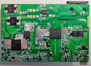
The design, DER-937, contains: specification, schematic, PCB layout, bill of materials, detailed magnetics specifications and performance data (inlcluding thermal performance).
“This USB PD charger design reaches efficiency levels in excess of 93%, including input, PFC and flyback stages,” said marketing engineer Aditya Kulkarni. “Its no-load performance is also excellent – the circuit requires less than 40mW at 230Vac.”


It uses the InnoSwitch3-PD INN3870C off-line quasi-resonant fly-back switcher, which combines a USB Type C and USB PD controller, a mains voltage gallium nitride switch, synchronous rectification and the company’s FluxLink inductive feedback.
For power factor correction (PFC) it has the HiperPFS-4 PFS7628C controller IC which “delivers greater than 98% efficiency across the full load range”, said the company.
A CapZero IC discharges the reservoir for safety when power is removed. There are 121 components in total.
It meets CISPR22 / EN55022 Class B conducted EMI, with >6dB margin at worst case (20V 5A 115Vac).
Without an enclosure it fits into 84 x 55 x 24mm, equating to 15W/in3.
DER-937 can be found here, from where the detailed pdf can be downloaded – Take a look as Power Integrations reference designs are among the best and, for example, include detailed magnetics winding instructions as well as thermal images and EMC plots. Ed.