Gallium nitride (GaN) power semiconductors are about less. Less CO2 emission from device fabrication, less materials in the devices and power converters using GaN, less cost due to higher frequency operation and smaller passive components, and less thermal dissipation due to higher efficiencies. Those performance factors combine to improve the sustainability of power converters built using GaN. Designers of all types of power converters need to keep updated on the numerous performance and cost benefits of using GaN.
This FAQ starts by looking at the challenges associated with reductions in emissions of greenhouse gases (GHG) like CO2, then looks at how GaN fits in beginning with lower emissions during device fabrication, including the use of AI for higher quality GaN substrates, the dematerialization resulting from the combined effects of the smaller die sizes of GaN devices compared with Si and the higher frequencies enabled by GaN, and the higher efficiency of GaN power converters that’s the icing on the cake further reducing lifetime GHG emissions.
The need
The International Renewable Energy Association (IRENA) has defined the increases in electrification and efficiency needed to support its “1.5 °C pathway.” The pathway requires new ways of producing and consuming energy and aims to reduce almost 37 gigatons (GT) in annual CO2 emissions by 2050. Developments required to enable moving forward on the pathway include (Figure 1):
- Increases in the generation and direct use of electricity from renewable energy sources.
- Improvements in energy efficiency.
- Increasing electrification of transportation and other end uses.
- Use of clean hydrogen and its derivatives.
- Use of bioenergy sources coupled with carbon capture and storage.
- Carbon capture and storage in the ‘last mile.’


As seen in the figure, increased use of renewables, higher energy efficiency, and growing electrification are expected to account for most of the gains. More efficient power converters based on GaN will be one of the keys to achieving those aggressive goals.
Smaller die
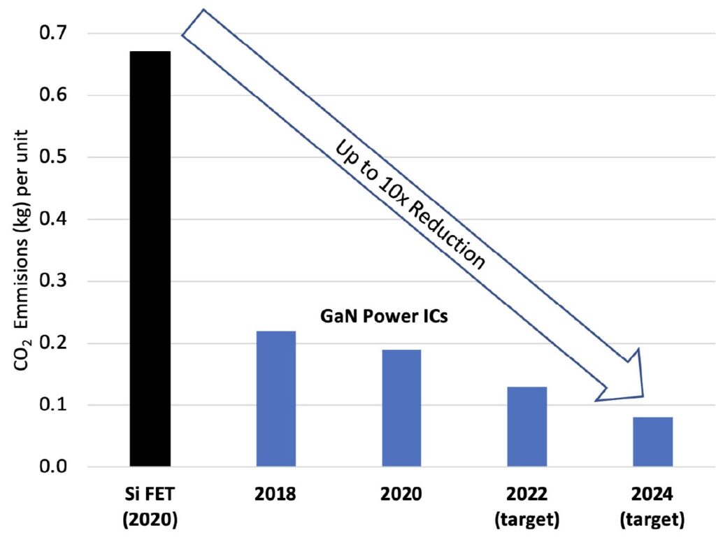
GaN die are smaller than comparable Si die. Smaller die mean less consumption of energy and chemicals and lower CO2 emissions per die. As of 2020, a production of a GaN power device produced 4x less CO2 compared to a Si FET, and the difference is expected to grow since Si is a mature technology and GaN is still evolving and improving with a new generation of devices every 12 to 18 months (Figure 2).

AI for GaN wafers
It’s not just the die getting smaller; the wafers on which the die are produced are getting better, leading to higher yields and driving down effective CO2 emissions even more. A deep learning epitaxy platform is being deployed that merges real-time AI-based image analysis of the wafer surface with hybrid molecular beam epitaxy (MBE) technology to produce better GaN wafers.
The imaging platform captures crystal structure information at the atomic layer level using reflection high energy electron diffraction (RHEED) imaging technology. The resulting information is analyzed in real time using deep learning and AI to control the hybrid MBE system and maximize wafer quality.
The imaging system observes changes at the sub-angstrom level and the AI learns the optimized diffraction patterns. The AI also monitors and controls the stresses and warpage of the wafer. The system controls the wafer fabrication process using a combination of condition monitoring, quality predictions, and precise changes in the production processes. In addition to improving wafer quality, the cost of GaN devices is falling due to the increasing use of 8-inch GaN-on-Si wafers, resulting in an absolute cost advantage compared to Si FET-based solutions.
Less material and money
Compared with Si FETs, GaN devices have a better figure of merit (FOM) that accounts for on state and switching performance like RDS(on) x QG, where RDS(on) is the on resistance, and QG is the total gate charge, including the integration of gate-source capacitance (CGS) plus gate-drain capacitance (CGD) over voltage. A better FOM means that GaN-based solutions can be smaller and lighter weight compared to solutions using Si FETs. For example, the hard-switching FOM of 80 to 100 V GaN devices is about 4x better than Si FETs, and GaN has a lower RDS(ON), which produces less thermal dissipation. GaN devices are smaller than Si FETs, 6x to 10x more thermally efficient, and can support power densities 10x or more, higher than Si FETs. The higher switching frequencies of GaN devices enables the use of fewer and smaller passive components, especially for input and output filtering, further increasing power densities.
As a result of the smaller passive components, less (or no) need for heat sinking, and smaller PCB area, GaN solutions are cost equivalent with Si FET designs in a growing number of applications (Figure 3). The longer-term trend favors increased GaN adoption. Si FETs are a mature technology experiencing only marginal increases in performance and power densities. As recently as 2021, GaN devices were about 300x larger than their theoretical limit, making continued reductions in GaN device size and cost inevitable.

eMobility and data center costs
The GaN advantage extends beyond the board-mounted dc/dc converters described above. It extends to multi kW power converters used in eMobility and data center applications like a 3 kW, 48 to 12 Vdc converter, as detailed in Figure 4. The left-hand green bar (100%) is the reference cost for a Si-based design in 2019, and the short white bar next to it (12%) is the portion of the cost attributable to the Si FET. The orange bar next to that (125%) is the cost for a comparable GaN-based dc/dc converter, also in 2019, and the white bar (40%) was the cost of the GaN device. This year, the situation is projected to change significantly. The costs for the Si-based power converter and the Si FET drop slightly, by 10% and 2%, respectively. The change is more dramatic for GaN where the power converter cost drops to parity with the Si-based design, 89% versus 90%, respectively, and the relative cost of the GaN device drops by half, from 40% to 20%. The GaN device still costs more than the Si FET, but the balance of the components are cheaper, leading to overall cost parity for the GaN- and Si-based power converters. In the future, GaN will have an absolute cost advantage over Si in these applications.


Higher efficiency
Even before GaN power converters reach price parity with Si designs, GaN offers significantly higher efficiencies. The reduced capacitances and circulating currents in GaN devices significantly impact the efficiency differences at light loads. At higher currents, the lower resistance of GaN devices results in higher efficiency, but the difference between GaN and Si is narrower (Figure 5). In most applications, cost parity is a mandatory condition for using GaN but is a one-time benefit. The benefits of higher energy efficiency, including reduced energy consumption, lower energy costs, and correspondingly lower GHG emissions, are enjoyed throughout the operating life of the converter.


For example, a wireless charging system for EVs with an efficiency of 96% was developed by the EU’s UlimatGaN project. Current commercial systems using Si devices have efficiencies of up to 93%. A 3% efficiency increase is projected to reduce CO2 emissions by about 1.7 megatons per year by 2030, the same amount of CO2 emitted annually by about one million cars with internal combustion engines. It’s been estimated that using GaN power converters can reduce CO2 emissions by up to 8 tons per year in a typical data center rack. Cloud data centers have tens of thousands of racks.
Summary
The use of GaN power devices will result in a dramatic reduction in GHG emissions. It’s one of the keys to achieving IRENA’s 1.5 °C pathway. The cost of using GaN is falling due to numerous factors, including the continual shrinking of GaN, die, the increasing size of GaN wafers, and increasing yields. As a result, GaN power converters are at or near price parity with Si-based power converters, and the GaN designs can reduce GHG emissions and long-term operating costs.
References
Enabler of Green Applications, EU UltimateGaN project
Energy-saving chips made of gallium nitride boost efficiency and CO2 savings, Infineon
Epitaxial growth artificial intelligence platform, IVworks
Sustainability Report 2021, Navitas Semiconductor
The GaN Breakthrough for Sustainable and Cost-Effective Mobility Electrification and Digitalization, MDPI electronics
World Energy Transitions: Outlook 2022, International Renewable Energy Agency