Silicon-carbide (SiC) mosfets have made significant inroads in the power Semiconductor industry thanks to a range of benefits over silicon-based switches. These include faster switching, higher efficiency, higher voltage operation, and higher temperatures that result in smaller and lighter designs. This has helped them find homes in a range of automotive and industrial applications. But wide bandgap (WBG) devices like SiC also introduce design challenges, including electromagnetic interference (EMI), overheating, and overvoltage conditions, which can be solved by choosing the right gate driver.
Since gate drivers are used to drive the power device, it is a critical piece of the power puzzle. One way to ensure an optimized design using SiC includes first carefully considering your choice of the gate driver. Simultaneously, it requires a close look at the key requirements of your design – efficiency, density, and, of course, cost – because there are always trade-offs, depending on the application requirements.
Despite the inherent benefits of SiC, pricing is still a roadblock to adoption. If you look at SiC versus silicon on a part comparison basis, it’s going to be more expensive and difficult to justify unless designers look at the total solution cost, according to power IC manufacturers.
So let’s first address the applications, benefits, and trade-offs of SiC versus silicon MOSFETs or IGBTs. SiC FETs offer lower on-resistance (thanks to a higher breakdown voltage), high saturation velocity for faster switching, and a 3× higher bandgap energy, which results in a higher junction temperature for improved cooling, and 3× higher thermal conductivity, which translates into higher power density.
There is industry agreement that low-voltage Si MOSFETs and GaN play in the <700-V range and above that is where SiC comes into play with a little bit of overlap in the lower power range.
SiC is mostly replacing silicon IGBT type applications over 600 V and above 3.3 kW, and even more so at about 11 kW, which is really more of a sweet spot for SiC, which means high-voltage operation, low switching losses, and a higher switching frequency power stage, said Rob Weber, product line director, digital gate driver (AgileSwitch), Discrete and Power Management, Microchip Technology.
This allows the use of smaller filters and passives and it reduces the cooling needs, he said. “We’re talking system-level benefits versus IGBTs, which is ultimately a reduction in size, cost, and weight.
“From a loss perspective, you can reduce the losses up to 70 percent, for example, at a 30-kHz switching frequency, and that is a result of some of the different characteristics of silicon carbide in terms of the breakdown field, electron saturation velocity, bandgap energy, and thermal conductivity,” said Weber.

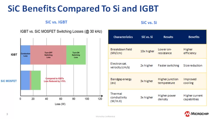
SiC vs. Si and IGBTs (Source: Microchip Technology)
The benchmark that engineers look at is efficiency, which results in levels of improvement, but the other thing that is happening more and more in SiC is the system-level benefits over IGBTs, said Weber.
“With silicon carbide you can operate at a higher switching frequency that enables you to have smaller external components that surround the immediate power stage like filters, for example, which are big, heavy magnetic devices; operate at higher temperatures or operate cooler due to the lower switching losses; replace a liquid-cooled system with an air-cooled system, and shrink the size of the heat sink,” he explained.
This component reduction in size and weight, which translates into lower cost, means that SiC goes way beyond getting better efficiency, he said.
However, in a part-to-part price comparison, SiC is still more expensive than traditional silicon-based IGBTs. “The SiC module will cost more from every manufacturer, but when you look at the total system, the SiC system costs are lower,” said Weber.
In an example shared by Weber, one customer was able to achieve a six percent reduction in system costs when using a SiC mosfet.
Once the designer has made the decision to switch to SiC, they also need to look at the trade-offs. Power semiconductor manufacturers agree there are “secondary effects” like noise, EMI, and overvoltage that have to be dealt with.
“When you’re switching these devices faster, you potentially create more noise which will translate into EMI,” said Weber. “In addition, while SiC is great at higher voltage it is also much less robust than IGBTs for short-circuit conditions and you’re getting variability in your voltage, so you get overvoltage conditions, which is causing some designers to use higher voltage rated SiC devices, so they can control the overvoltage better and overheating.”
This is where the selection of the gate driver plays a big role. SiC has unique requirements for characteristics such as supply voltage, fast short-circuit protection, and high dv/dt immunity.
Selecting the SiC gate driver
When it comes to selecting the right gate driver for SiC switches, it takes a new mindset in thinking about the power solution compared to silicon-based devices. The key areas to look at include topology, voltage, bias, and monitoring and protection features.
The selection of the gate driver is vital, and historically it was okay to use a sequential approach to selecting the gate driver, said Weber. “Prior to SiC you’d pick the IGBT first then the gate driver second then the busbars and the capacitor, etc.,” said Weber. “It’s totally changed. You have to look at the whole holistic solution that you’re building and those tradeoffs at every step instead of this sequential approach that you have with IGBTs. It’s been an education for a lot of customers.”
In addition, there are a variety of gate drivers for SiC that range in features and integration (and price), targeting simple to more complex designs.
As an example, Analog Devices Inc. (ADI) organizes its gate drivers by class – basic functions, “protecting” with protection features such as overcurrent protection and fault detection, and full programmable configurability. ADI’s isolated gate drivers are based on the company’s iCoupler isolation technology combined with high-speed CMOS and monolithic transformer technology, which delivers ultra-low propagation delay without sacrificing common-mode transient immunity (CMTI) performance, according to the company. ADI also offers a portfolio of evaluation boards and reference designs that provide a good starting point for product design.
Topology, power level, protection and functional safety requirements, and the generation of SiC device in use will dictate the kind of driver needed for the application, said Lazlo Balogh, system engineering lead, high voltage power, Texas Instruments Inc.
For example, a non-isolated driver, which could require a lot of extra circuitry, is good for simpler applications, where not everything has to be integrated into the driver, he said.
There are also isolated drivers that can handle the negative bias and isolation issues but will still need some kind of monitoring in the system, up to devices that offer further integration such as monitoring and protection circuitry and functional safety for automotive applications, he added.
“The checklist for deploying SiC the right way is to look at the topology and what kind of devices you have to drive then pick the gate driver, optimize the bias, figure out what kind of protection is needed, and then optimize the layout,” Balogh said.
From a driver point of view, it’s having the right bias, so the right voltage capability, whether you need isolated or non-isolated gate drivers, how much protection is needed, which ties into the integration level [for protection and safety] or how much extra circuitry is required, he added.
One of the things that has hindered SiC a little bit is the realization that, because of the higher switching speed, it needs to be put into a package where the source inductance is eliminated, which is typically done with the Kelvin source connection, said Balogh. “Source inductance can be nasty and cause a lot of ringing and additional power losses because it slows down the switching action.”

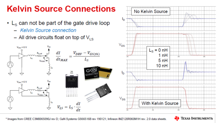
Kelvin source connections. Click for a larger image. (Source: Texas Instruments Inc.)
“This is where the layout engineer becomes your best friend because you really have to look at the layout to mitigate the ringing and optimize it for high speed switching,” said Balogh. This includes minimizing the trace inductances and separating the gate loop from the power loop and proper bypassing [of the switched current path and broad frequency band] by selecting the right components, he added.
What’s really critical is connecting the driver to the switch, Balogh said. You have to connect the ground of the driver directly to the source of the power switch because of stray inductances that can increase switching losses, he said.
Texas Instruments offers a number of reference boards/designs that gets the customers close to their performance requirements. There are always little tradeoffs and TI can help them optimize their designs based on their needs, such as if they need peak efficiency at full load, Balogh said. His advice: Read the application notes and contact the application engineers if you have any concern driving WBG.
TI offers a range of Si and IGBT gate drivers, including the UCC21710, UCC21732, and UCC21750. These are isolated gate drivers with integrated protection and sensing features. The devices provide fast detection time to protect against overcurrent events while ensuring safe system shutdown.

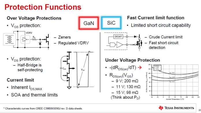
Protection functions. Click for a larger image. (Source: Texas Instruments)
Mladen Ivankovic, regional applications engineer, Infineon Technologies, said when selecting a SiC MOSFET the first critical question to ask is ‘do I need unipolar or bipolar driving’ for that component.
There are fast and robust drivers in the market that can drive both Si as well SiC but what people need to be cautious about when moving from Si to SiC is how you drive it because silicon is driven with a typical voltage of 12 volts, Ivankovic said. “You are using 12-V to turn-on and using 0 V to turn-off, so the normal voltage range for the driver driving silicon components or superjunction MOSFETS is 0 to 12 volts and that’s across the board from any silicon component supplier, he added.
On the other hand, SiC devices from different vendors will have different turn-on/turn-on voltages. There are SiC MOSFETs in the market, for example, that require +15 V to turn it on and -4 V to turn it off, or +20 V for turn-on and -2 or -5 V for turn-off, Ivankovic said. “This requires a driver that enables the use of positive and negative voltages.”
But with an Infineon SiC, you’ll only need a wider voltage range, he said. “So instead of 0 to 12 V, you’ll need to drive it with 0 to 18 V and you can use the same driver that is used for Si or SiC.”
So you have to be careful about whether you need a unipolar gate driver or you need both a positive and negative to drive the component properly, Ivankovic said.
Infineon recently introduced the EiceDRIVER X3 Enhanced analog (1ED34xx) and digital (1ED38xx) gate driver ICs for a range of industrial applications. Both families are designed for IGBTs as well as Si and SiC MOSFETs in discrete and module packages. The 1ED34xx offers an adjustable desaturation filter time and soft turn-off current with external resistors and the 1ED38xx provides I2C configurability for multiple parameters, including adjustable control and protection functions such as short-circuit protection, soft-off, undervoltage lockout, a Miller clamp, overtemperature shutdown, and two-level turn off (TLTO).


Infineon’s EiceDRIVER 1EDBx275F is a family of single-channel isolated gate-driver ICs that is designed to drive Si, SiC, and GaN power switches. (Source: Infineon Technologies)
Another gate driver consideration is peak current capacity capabilities, according to Eric Benedict, senior applications engineer, at ADI, which he covered in a training session webinar with Wolfspeed. “So why is that an important feature in driving the switches? In most cases it’s going to come down to efficiency in the form of reduced switching losses. In order to complete the switching transition the gate needs to deliver enough charge to the gates so the switch is fully on. Speeding up the switching means delivering this charge faster and since current is charge versus time, faster switching means more gate drive current. Thus the peak drive current is going to be determined by the gate supply voltage in the total resistance in the gate loop.”
Benedict’s caveat when looking at data sheets is that manufacturers report their gate driver output currents based on different test conditions. “Some specify currents that are retrieved during a very short circuit pulse where you short the output while others use currents that are measured when you have some realistic gate resistance that are present, so you do need to be careful when comparing specs from the different devices.”
Some of the key points covered in the training session include the importance of selecting a gate driver that has sufficient drive capability to take advantage of the switching frequencies to bring down the losses, providing proper immunity to common-mode transients, focusing on the layout so it is tuned for SiC, such as minimizing parasitics, and understanding that the desaturation or short circuit protection is different from an IGBT.
Configurable digital gate drivers
Many leading power IC manufacturers have developed unique SiC gate driver technologies and solutions to address some of the secondary effects as well as to maximize the benefits of making the switch to a WBG technology.
Microchip, for example, takes a digital approach with its AgileSwitch drivers, which includes a unique technique called “Augmented Switching.” A key element of this technique is the configurable turn-on/turn-off, offering a series of steps that controls the voltage levels and the time at those voltage levels. This allows designers to configure the turn-on/turn-off profiles digitally through software, eliminating the need to make changes in hardware. The technique also includes additional levels of fault monitoring detection and short circuit response.
Microchip claims significant improvements: up to 50 percent lower switching losses and 80 percent lower voltage overshoot.
“A traditional analog approach is certainly fine for silicon switches, where a lot of these secondary effects weren’t issues in driving a slow IGBT but silicon carbide is an entirely different animal,” Weber said.
One of the key elements of the digital gate driving technology is protecting a short circuit condition very quickly and then responding to it in a safe manner, said Weber.

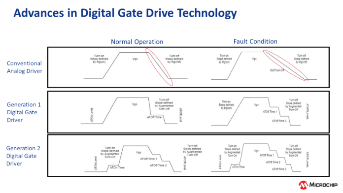
Advances in digital gate drivers (Source: Microchip Technology)
Microchip recently introduced its Generation 2 digital gate driver that added new levels of control over the first-generation devices. The configurable gate drivers can be used with any supplier’s SiC MOSFETs.
The differences in the MOSFETS have to do with the turn-on and turn-off voltages, so the ability to program the +/- voltage levels even when company to company they might have different positive and negative voltages, these are all configurable through the gate driver, Weber said.
AgileSwitch configurability. Click for a larger image. (Source: Microchip Technology)
Weber said customers have been able to reduce their development cycles and development time by up to six months. “The idea that you can use software to do things that you used to do with the soldering gun or board re-spins is a different mindset. But you know for the customers who have started to adopt it they consider it game-changing.”
He also noted it gives customers more flexibility particularly during times of supply chain challenges. “Companies will be able to move between suppliers as supply is available.”
Microchip implements the ASD2 digital gate driver IC in a series of gate driver board products, which are referred to as gate driver cores – half-bridge devices with power supply gate drivers with a microprocessor and some level of configurability and control. The company also supports industry-wide compatibility with a line of adapter boards or daughtercards that enables the use of different industry-standard module types that both Microchip and competitors offer.
The digital gate driver also allows designers to optimize the MOSFET for today’s application instead of optimizing for five or 10 years out to account for switch degradation over time or use.
“With our drivers one of the things that customers are looking at and are interested in is the ability to optimize for the MOSFET today with the idea that over time if the MOSFET does degrade they can change the settings to optimize around the MOSFET. In this way, they get more efficiency out of the the system today and not give up that efficiency by designing for a future worst case,” said Weber.
This can be done in an analog solution and there are always multiple ways to get there but what are the costs, tradeoffs, and time spent to develop the solution, he added.
Using standard drivers
Suppliers agree that it is possible to use standard drivers to control the SiC devices but they have to decide on the magnitude of the tradeoff and that tradeoff usually entails extra circuitry or larger external devices. As an example, one way to reduce ringing and overvoltage when using a standard driver is by increasing the size of the gate Resistor.
Balogh noted other issues that need to be considered such as protection functions, undervoltage lockout, higher frequency operation, faster switching, and hot spots on the die, which all can have an impact on power losses, EMI, and size.
In addition, the extra circuitry usually takes much more space than an integrated solution and dedicated SiC, so there are a lot of negatives, and for that reason higher end designs opt for a dedicated SiC core driver, which takes into account things like faster switching, overvoltage conditions, and issues around noise and EMI, he said.
“You always can use a standard gate driver but you have to complement it with additional circuitry and usually that is the trade-off,” said Balogh.
As an example, for a small high-power-density design a standard non-isolated gate driver in a SOT23 package can be used, said Balogh. Non-isolated drivers aren’t directly applicable but it can be done and a lot of people take this path, he said.
about Analog DevicesInc.Infineon TechnologiesMicrochip TechnologyTexas Instruments