
The move adds to its sustained production capacity for 100mm, 125mm and 150mm bonded wafers and advanced engineering substrates.
“We are the last man standing for the manufacturing of 100mm SOI and SiSi direct bonded wafers and we seen have a shift in the industry away from production of 125mm, 150mm, and now 200mm’” says IceMOS founder and chairman Sam Anderson, “instead of issuing end-of-life notices, we are an established, trusted manufacturer that is here to stay.”
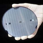
200mm bonded substrates from IceMOS are used as a starting material for MEMS such as pressure sensors, inertial MEMS and optical MEMS, including micro-mirrors for AR/VR and LiDAR applications.
As the automotive industry moves towards greater electrification, so the industry requirement increases for environmental, inertial and optical MEMS sensors and IceMOS intends to service this rise in demand from the MEMS and analogue IC industry.
IceMOS has committed to support the demand for 100mm, 125mm and 150mm bonded SOI and SiSi wafers and advanced engineering substrates (including cavity bonded), while other suppliers shift to larger diameters.
Several device manufacturers with applications in MEMS and discrete Semiconductor applications have well established production lines and qualified process flows that require small diameter SOI and SiSi.
“Our customers have already committed to 100mm or 150mm diameter dedicated equipment, with specialized process flows and inspection techniques that satisfy the requirement for high sensitivity automotive, aerospace, lifestyle and medical applications, among others,” says IceMOS sales chief Hugh Griffin, “availability of small diameter bonded wafers will enable the on-going development of new sensing technology as well as production of legacy products for many years to come.”