
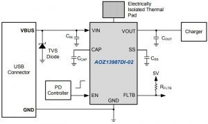
There are two: AOZ13984DI-02 and AOZ13987DI-02, both in 3 x 3mm thermally-enhanced DFN packaging, designed to be used in devices that are charged through a USB connector, to prevent current flowing back out of the device through the Vbus pin.
Inside is a control IC co-packaged with back-to-back mosfets, and reverse current under fault conditions can be blocked while working at up to 22V.
The differences are:
- AOZ13984DI-02: 33mΩ typical on-resistance, 5.5A continuous sink, 15A peak (10ms 2% duty)
- AOZ13987DI-02: 20mΩ typical on-resistance, 8A continuous sink, 20A peak (10ms 2% duty)
In both cases, normal operation is over 3.4 to 22V (28V abs max) and -40 to +125°C junction (thermal resistance is 2.8°C/W θjc and 36°C/W θja).
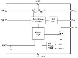

If for any reason Vout increases such that Vin – Vout is <35mV, it is assumed that current is about to be forced back through the IC and the gate driver forces the switch to turn off.
A fast comparator also turns off the power switch if Vout – Vin is higher than 50mV after a delay time. And when it is first enabled, or during auto-restart, the power switch will be kept off if Vout is 50mV higher than Vin, according to the data sheets.
The switch is also turned off when the die reaches 140°C, after which it can only be re-enabled by either toggling the enable pin or cycling the input power supply.
Soft-on is implemented, so when device is enabled thorough its enable pin, the mosfet gates are controlled to ramp the output up linearly until Vout reaches Vin at a rate set by an external capacitor.