Historically, industrial field sensors were and still are in many cases analog. They include a sensing element and some way to get the sensing data to a controller. Data was unidirectional analog. Then came binary sensors, which provided a digital on/off signal, and included a sensing element: inductive, capacitive, ultrasonic, photoelectric, etc. with a Semiconductor switching element. The output could be high-side (HS) switching (PNP) or low-side (LS) switching (NPN) or push-pull (PP). But data was still limited to unidirectional communication from the sensor to the master, had no error control, and still required a technician on the factory floor for tasks such as manual calibration.
A better solution was needed to meet the demands of “Industry 4.0”, smart sensors, and reconfigurable factory floors. The solution is the IO-Link protocol, a relatively new standard for industrial sensors that is showing a phenomenal growth trajectory.
The IO Link organization estimates that over 16 million IO-Link enabled nodes are being used in the field to date. That number is still growing.

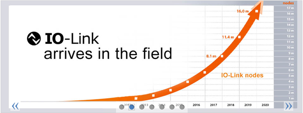
Fig. 1: IO-Link protocol’s rapid growth (Image: IO-Link Consortium)
IO-Link is a standardized technology (IEC 61131-9) that regulates how sensors and actuators in industrial systems interact with a controller. IO-Link is a point-to-point communication link with standardized connectors, cables, and protocols. The IO-Link system is designed to work within the industry standard 3-wire sensor and actuator infrastructure and comprises an IO-Link master and IO-Link device products.
IO-Link communication is between one master and one device (sensor or actuator). Communication is binary (half-duplex) and is limited to 20 m, using unshielded cables. Communication requires a 3-wire interface (L+. C/Q, and L-). The supply range in an IO-Link system is 20 V to 30 V for the master and 18 to 30 V for the device (sensor or actuator).
Maxim’s IO-Link handbook1 elaborates IO-Link advantages as follows:
“IO-Link is a technology that enables a traditional binary or analog sensor to become an intelligent sensor that no longer just gathers data but allows a user to remotely change its settings based on real-time feedback obtained on the health and status of other sensors on the line, as well as the manufacturing operation it needs to perform. IO-Link technology enables sensors to become interchangeable through a common physical interface that uses a protocol stack and an IO Device Description (IODD) file to enable a configurable sensor port. It is truly plug-and-play ready while providing the ability to reconfigure parameters on-the-fly.”
Within the factory network hierarchy, the IO-Link protocol sits at the edge, which are typically sensors and actuators as shown in Fig. 2. Many times, the edge devices communicate to a gateway that translates the IO-Link protocol to the fieldbus of choice.

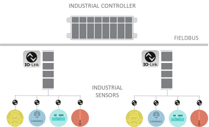
Fig. 2: IO-Link protocol is used to connect intelligent edge devices to the factory network. (Image: Maxim Integrated)
For more information on how IO-Link enables next-generation manufacturing environments or Industrial IoT (as it is sometimes called), refer to a previous article that explains this in detail2.
Designing IO-Link sensors
Industrial field sensors must be rugged, small, and very energy efficient so that the heat dissipation is kept to a minimum. Most IO-Link sensors have the following components:
- Sensing element with the associated analog front end (AFE)
- A microcontroller that processes data, and in the case of an IO-Link sensor, also runs the lightweight protocol stack.
- An IO-Link transceiver that is the physical layer.
- Power supply and in many cases protection (TVS for surge, EFT/burst, ESD, etc.).
Recommended
Intelligence at the factory edge: Boost productivity and improve costs
Heat dissipation (power efficiency)
Once we understand the typical components, we can look at how a hypothetical sensor power is budgeted. See Fig. 3. All of these numbers are estimates. They show that the transceiver (output stage) power consumption matters when budgeting the total system power consumption of a sensor.
Let‘s start at the left-most side, which specifies an older generation of IO-Link sensor. That way it becomes clearer how advances in technology in the microcontroller (MCU) and the output stage (i.e., the transceiver) has contributed to the lowering of the total system power over the years.
Original or first generation IO-Link transceivers consumed 400 mW or higher. The newest low-power Maxim IO-Link tranceivers consume less than 100 mW. Also, the MCUs have helped. A legacy MCU consumes as much as 180 mW, but the newer low-power MCU can go down to 50 mW.
A state-of-art IO link transceiver coupled with a low-power MCU can keep the total sensor power budget in the range of 400 mW to 500 mW.
Power dissipation is directly related to heat dissipation. The smaller the sensor the more stringent the power dissipation specification. By some estimates, an 8-mm diameter (M8) enclosed cylindical IO-Link sensor will specify a maximum power dissipation of 400 mW and a 12-mm diameter (M12) enclosed cylindical IO-Link sensor will specify a maximum power dissipation of 600 mW.
And the technology keeps getting better. One of the new IO-Link transceivers from Maxim Integrated, the MAX14827A, dissipates a remarkably low 70 mW when driving a 100 mA load. This is achieved by optimizing the technology to deliver a very low 2.3 Ω (typ.) RON (on-resistance).

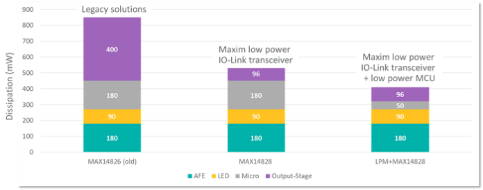
Fig. 3: A hypothetical IO-Link industrial sensor power budget. (Image: Maxim Integrated Products)
For sensors that use very low operating current, say 3 to 5mA, and require a 3.3-V and/or a 5-V supply; the regulated power can be sourced via an LDO. And indeed, Maxim’s IO-Link transceivers have included an integrated LDO. But as the current demand increases to say 30 mA, the LDO will soon become the dominant source of power/heat dissipation in the system. To compare at 30 mA, the power consumption of an LDO can be as high as 600 mW.
LDO Power @30 mA = (24-3.3) x 30 mA = 621 mW
In comparison, a DC-DC buck converter supplying a 30 mA sensor with a 3-V output voltage will dissipate just 90 mW. Assuming the converter is 90% efficient (just 9 mW power loss), the overall power consumption is just 90 + 9 = 99 mW 3.
Maxim’s newest IO-Link transceivers have integrated a high-efficiency DC-DC regulator as shown in Fig. 4.

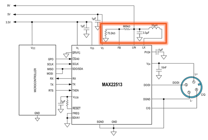
Fig 4: Maxim’s newest MAX22513 IO-Link transceiver incorporates an integrated high efficiency DC-DC regulator. (Image: Maxim Integrated Products)
Size of the IO-Link sensor
After heat dissipation, size is the next biggest concern for all industrial sensors, and it applies as well to the new IO-Link sensors. Board space becomes increasingly at premium as we migrate to a smaller form-factor.
Fig. 5 shows that for a 12-mm diameter housing, the transceiver in a wafer level package (WLP) and the DC-DC can sit side by side on a regular PCB which has 10.5-mm width. There is still room for vias and wires on the same side. If the sensor housing is 6 mm, then the PCB width is down to 4.5 mm. Then the chips must be mounted on both sides of the PCB even with small WLP packages.

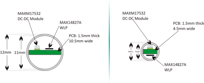
Fig 5: Size is another big issue in the newest IO-Link sensor designs. (Image: Maxim Integrated Products)
To enable these sizes, the transceiver must be available in a WLP that allows for the smallest size. This size limitation is also one of the reasons we have integrated a DC-DC inside our newest IO-Link transceiver as shown before.
But most industrial sensors also must be designed to work in a rugged environment, which means they must incorporate protection circuitry such as TVS diodes, which are not shown in Fig. 5. This is where it is important to pay attention to the absolute maximum ratings specification for the IO-Link transceivers.
Let’s elaborate: Why do 65-V absolute maximum ratings on the IOs reduce the size of the sensor subsystem? Typically, the sensor needs to survive surge pulses between the 4-pins: GND, C/Q, DI, and DO. Maxim’s IO-Link transceivers have a spec of 65-V absolute maximum ratings. If we take an example of a 1 KV at 24 V surge between C/Q and GND.
Voltage between C/Q and GND = TVS clamp voltage + TVS forward voltage
With the higher absolute maximum ratings specification, the designer can use a small TVS diode such as the SMAJ33 whose clamp voltage is 60 V at 24 A and TVS forward voltage is 1 V at 24 A.
Voltage between C/Q and GND = 61V
This value above is within the absolute maximum ratings specification of the Maxim transceiver.
However, if the absolute maximum ratings specification is lower, typically in the industry it is around 45 V, then a much larger TVS diode such as the SMCJ33 is required to clamp the voltage down to an acceptable level. This diode is more than 3× the size than the one required for the Maxim transceiver.
The size impact of a larger TVS diode in the overall sensor design is significant if the transceiver’s absolute maximum ratings specification is lower. Table 1 shows an estimated difference in the PCB area. The assumption here is that the sensor must be able to withstand a high-level surge of ±1 KV/24 A.

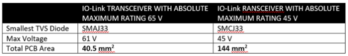
Table 1: Advantages of a 65-V absolute maximum rating on sensor size (Image: Maxim Integrated Products)
The next generation of IO-Link transceivers have even improved upon this. The newer IO-Link transceivers from Maxim now feature an integrated protection on IO-Link line interface pins (V24, C/Q, DI, and GND). All pins feature integrated ±1.2 kV/500 Ω surge protection. In addition, all pins are also reverse-voltage protected, short-circuit protected, and hot-plug protected.
Even with all the integrated protection features as well as the integrated DC-DC buck regulator, these devices are available in a tiny WLP package (4.1 x 2.1 mm); enabling a small IO-Link sensor design.
Conclusion
The first-generation IO-Link transceiver technology came in easy-to-use TQFN packages with integrated LDOs that would meet the needs of a small sensor design. As power and size considerations mounted, the second-generation transceiver technology optimized power consumption by moving to a technology that gave us lower RON to further reduce power consumption and were made available in even smaller WLP packages.
The newest generation of transceivers recognizes the need to integrate both the protection and a high-efficiency DC-DC buck regulator to further reduce the size and the heat dissipation of the sensor subsystem. Fig. 6 shows a high-level progression of the IO-Link transceiver technology from Maxim Integrated.

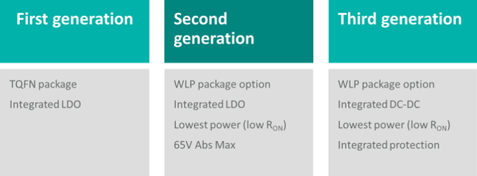
Fig. 6: Progression of IO-Link transceiver technology (Image: Maxim Integrated Products)
As IO-Link technology gets deployed in even more industrial sensors, these device specifications are key to implement small, ruggedized, power-efficient sensors.
1 https://www.maximintegrated.com/content/dam/files/design/technical-documents/handbooks/io-link-handbook.pdf
2 https://www.eletimes.com/io-link-enables-industrial-iot
3 https://www.maximintegrated.com/en/design/technical-documents/app-notes/6/6908.html
about Maxim IntegratedMaxim Integrated Products