“This article first introduces the semiconductor manufacturing process and the equipment and materials required, and then expounds the seven main production areas of the IC wafer production line and the required equipment and materials. Finally, the Semiconductor manufacturing process is introduced in detail. Take a look.
“
This article first introduces the Semiconductor manufacturing process and the equipment and materials required, and then expounds the seven main production areas of the IC wafer production line and the required equipment and materials. Finally, the semiconductor manufacturing process is introduced in detail. Take a look.
1. The semiconductor manufacturing process and the equipment and materials required
The processing process of semiconductor products mainly includes wafer manufacturing (Front-End) and packaging (Back-End) testing. With the penetration of advanced packaging technology, there is a process between wafer manufacturing and packaging. The link is called the Middle-End. Due to the many processing steps of semiconductor products, a large amount of semiconductor equipment and materials are required in the manufacturing process. Here, we use the most complex wafer fabrication (front-end) and traditional packaging (back-end) processes as examples to illustrate the equipment and materials required for the manufacturing process.


Integrated circuit Industry Chain
The wafer production line can be divided into 7 independent production areas: diffusion (Thermal Process), lithography (Photo-lithography), etching (Etch), ion implantation (Ion Implant), thin film growth (Dielectric DeposiTIon), polishing (CMP) , Metallization (MetalizaTIon). These 7 main production areas and related steps and measurements are all performed in the wafer clean room. Several kinds of semiconductor equipment are placed in these production areas to meet different needs. For example, in the photolithography area, in addition to the photolithography machine, there will also be matching glue/development and measurement equipment.
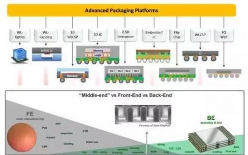
Advanced Packaging Technology and Middle-End Technology

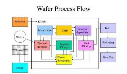
IC Wafer Manufacturing Flowchart


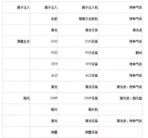

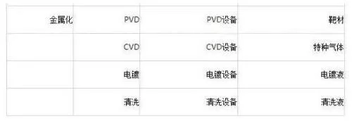

2. The 7 main production areas of the IC wafer production line and the required equipment and materials

Traditional packaging process

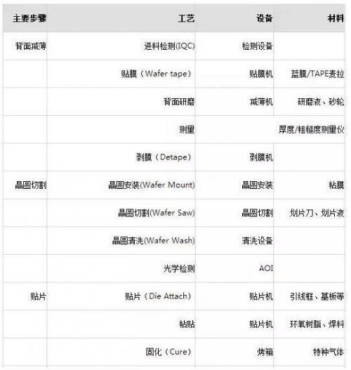
The traditional packaging (back-end) testing process can be roughly divided into 8 main steps, such as backside thinning, wafer dicing, placement, wire bonding, molding, electroplating, rib cutting/forming, and final testing. Compared with IC wafer manufacturing (front-end), back-end packaging is relatively simple, with lower technical difficulty, and the requirements for process environment, equipment and materials are much lower than wafer fabrication.


3. The main steps of traditional packaging and the required equipment and materials
The traditional packaging (back-end) testing process can be roughly divided into 8 main steps, such as backside thinning, wafer dicing, placement, wire bonding, molding, electroplating, rib cutting/forming, and final testing. Compared with IC wafer manufacturing (front-end), back-end packaging is relatively simple, with lower technical difficulty, and the requirements for process environment, equipment and materials are much lower than wafer fabrication.


4. Analysis of semiconductor manufacturing process
The semiconductor manufacturing process is the means for the realization of integrated circuits and the basis for the design of integrated circuits. Since the invention of the Transistor in 1948, the development of semiconductor device technology has gone through three main stages: in 1950, the alloy process was used to produce a practical alloy junction Transistor for the first time; in 1955, the diffusion technology was adopted to manufacture semiconductor devices. The major development of technology has opened up a new way for the manufacture of high-frequency devices; the emergence of planar technology and epitaxy technology in 1960 is a major change in semiconductor manufacturing technology, which not only greatly improves the frequency and power characteristics of the device, but also improves the stability of the device. It also makes the industrialized mass production of semiconductor integrated circuits a reality. At present, the planar process is still the mainstream process for the production of semiconductor devices and integrated circuits.
During the first 35 years of semiconductor manufacturing process development, feature size reduction was a hallmark of semiconductor technology development, with effective scaling-down efforts focused on increasing device speed and integrating on chips with acceptable yields More devices and features to improve performance. However, when the semiconductor industry evolves to the 45nm node or smaller, the scaling of devices will cause huge technical challenges. Two of the challenges are increasing static power consumption and inconsistency in device characteristics. These problems are about to reach the physical limit determined by atomic theory and quantum mechanics in CMOS technology.

Integrated circuit manufacturing is to perform a series of complex chemical or physical operations on silicon wafers. In short, these operations can be divided into four basic categories: thin film fabrication (1ayer), imprinting (pattern), etching and doping. These techniques of making transistors and fabricating interconnects on a single chip combine to form a semiconductor manufacturing process.
1. Photolithography process
Photolithography is the process of removing specific parts of the thin film on the surface of a wafer through a series of production steps. After this, a thin film with micro-patterned structures remains on the wafer surface. The removed portion may be in the form of a hole in the film or a remaining island-like portion. The goal of lithographic production is to generate dimensionally accurate features according to the requirements of the circuit design, in the correct location on the wafer surface, and in the correct relationship to other components. Through the photolithography process, part of the feature pattern is finally retained on the wafer. The photolithography process is sometimes called Photomasking, Masking, Photolithography or Microlithography, and is the most critical in the semiconductor manufacturing process. Errors made during the lithography process can cause distortion or poor registration, which can ultimately translate into an impact on the electrical properties of the device.
2. Doping process
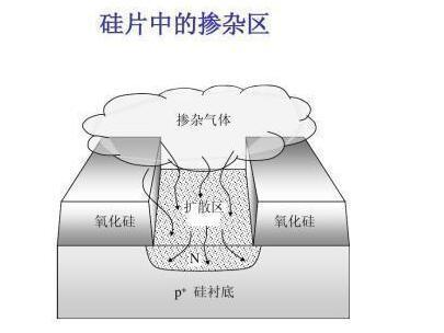

Doping is the process of introducing specific amounts of impurities into the surface of the wafer through film openings. It can be achieved in two ways: thermal diffusion and ion implantation. Thermal diffusion is a chemical reaction that occurs at a high temperature of around 1000°C, and the wafer is exposed to the gaseous state of certain doping elements. A simple example of diffusion would be the release of deodorant from a pressurized container into a room. The dopant atoms in the gaseous state migrate to the exposed wafer surface through diffusion chemical reactions, forming a thin film. In chip applications, thermal diffusion is also known as solid-state diffusion because the wafer material is solid. Thermal diffusion is a chemical reaction process. And ion implantation is a physical reaction process. The wafer is placed on one end of the ion implanter, with a source of dopant ions (usually gaseous) on the other end. At one end of the ion source, the dopant atoms are ionized (with a certain charge) and applied to ultra-high speed by an electric field, passing through the surface of the wafer. The momentum of the atoms injects the dopant atoms into the surface of the wafer, like a bullet shot from a gun into a wall. The purpose of the doping process is to create pockets in the wafer surface, either electron-rich (N-type) or hole-rich (P-type). These pockets form the PN junction of the electrically active region, on which the transistors, diodes, Capacitors, and resistors in the circuit all work.
3. Film layer growth process
Many thin films are created on the wafer surface, which can be insulators, semiconductors or conductors. They are composed of different materials and are grown or deposited using a variety of processes. These main process techniques are growing silicon dioxide films and depositing thin films of different materials. Common deposition techniques are chemical vapor deposition (CVD), evaporation and sputtering.
4. Heat treatment process
Thermal processing is the process of simply heating and cooling the wafer to achieve a specific result. During the thermal process, nothing is added or subtracted from the wafer, and some contaminants and moisture evaporate from the wafer. There is an important heat treatment step after the ion implantation process. The wafer damage caused by the implantation of dopant atoms will be repaired by heat treatment, which is called annealing, and the temperature is generally around 1000°C. In addition, there is a heat treatment step after the metal wires are fabricated on the wafer. These wires carry current between the various components of the circuit. To ensure good electrical conductivity, the metal is tightly fused to the wafer surface after heat treatment at 450°C. A third use of thermal processing is to heat the photoresist on the wafer surface to evaporate the solvent, resulting in precise patterns.
The Links: LM215WF3-SLL1 LM215WF3-SDB1