“Engineers at the Massachusetts Institute of Technology (MIT) reported that they created the first high-quality films in a new series of Semiconductor materials. The lead researcher of the study, Rafael Jaramillo, called this feat his “white whale” because he has been pursuing this feat for many years, and if history repeats itself, it may affect multiple technical fields.
“
Engineers at the Massachusetts Institute of Technology (MIT) reported that they created the first high-quality films in a new series of semiconductor materials. The lead researcher of the study, Rafael Jaramillo, called this feat his “white whale” because he has been pursuing this feat for many years, and if history repeats itself, it may affect multiple technical fields.

The ability to create high-quality thin films of other series of semiconductors has brought about the emergence of computers, solar cells, night vision cameras, etc.
Jaramillo pointed out that when a new material is introduced, the most important scientific breakthrough can only be achieved when the highest quality material can be obtained. “Researching low-quality materials often leads to false denials of their scientific interest and technological potential.”
In addition, he said that this new semiconductor family, so-called chalcogenide perovskites, can be used in solar cells and lighting. However, he pointed out that the history of semiconductor research shows that new semiconductor families are usually launched in unpredictable ways.


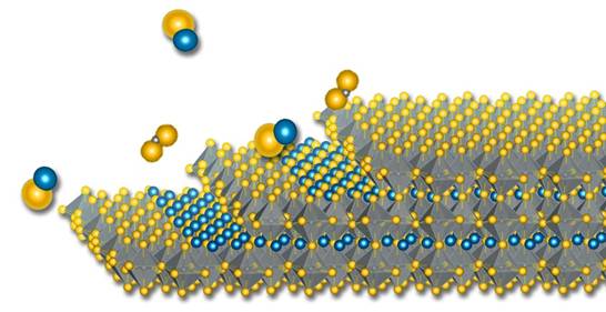
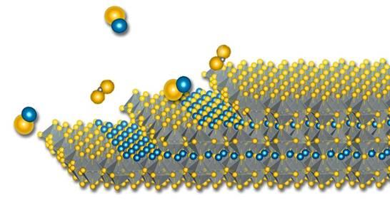
Because the new material has ultra-stable capabilities and is made of cheap, non-toxic elements, Jaramillo is excited about its potential. It is reported that the film created by Jaramillo’s team is composed of barium, zirconium and sulfur. It has a specific crystal structure, which is a typical brass compound peroxide. “You can make changes by changing the ingredients. Therefore, it is really a family of materials, not just one-offs,” Jaramillo said.
This work has been published in Advanced Functional Materials on November 3, 2021. Jaramillo’s co-authors include Ida Sadeghi, a postdoctoral fellow in the Department of Materials Science and Engineering (DMSE) and the first author of the paper, Kevin Ye, Michael Xu and Yifei Li, graduate students of DMSE, and James M. LeBeau, associate professor of John Chipman in the Department of Materials Science and Engineering at MIT.
It is understood that Jaramillo and colleagues use a technique called molecular beam epitaxy (MBE) to grow their high-quality thin films. This technology allows atomic-level control of crystal growth, but this is difficult to do and does not guarantee the success of the new material. Jaramillo pointed out that despite this, the history of semiconductor technology shows the value of developing MBE, “This is why it is worth a try.”
As its name implies, MBE essentially directs a molecular beam to a specific arrangement of atoms on the surface. This arrangement of atoms provides a template for the ejected molecules and allows them to grow on it. “This is why epitaxial growth can provide you with the highest quality films. These materials know how to grow,” Jaramillo said.
Another factor has further exacerbated the difficulty of this work. Jaramillo pointed out that the manufacture of this kind of chemicals is very difficult, they will smell and make the equipment sticky. MBE needs to be carried out in a vacuum chamber, but Jaramillo recalled that they were not entered into the vacuum chamber at that time.
Hideo Hosono, a professor at Tokyo Institute of Technology who was not involved in the research, said: “The film (created by Jaramillo et al.) shows a mirror-smooth image. This is the result of the atomically flat surface and the quality is very good. We can predict , The realization of equipment manufacturing such as solar cells and green LEDs will be the next target.”
Currently, Jaramillo’s group is focusing on two areas: exploring basic issues to gain a better understanding of materials, and integrating them into solar cells.
Although the halide perovskite is not the only focus of Jaramillo in the MIT laboratory. “But this is definitely the project we are most proud of because it took the most effort and the most delayed gratification,” Jaramillo said.
Engineers at the Massachusetts Institute of Technology (MIT) reported that they created the first high-quality films in a new series of semiconductor materials. The lead researcher of the study, Rafael Jaramillo, called this feat his “white whale” because he has been pursuing this feat for many years, and if history repeats itself, it may affect multiple technical fields.
The ability to create high-quality thin films of other series of semiconductors has brought about the emergence of computers, solar cells, night vision cameras, etc.
Jaramillo pointed out that when a new material is introduced, the most important scientific breakthrough can only be achieved when the highest quality material can be obtained. “Researching low-quality materials often leads to false denials of their scientific interest and technological potential.”
In addition, he said that this new semiconductor family, so-called chalcogenide perovskites, can be used in solar cells and lighting. However, he pointed out that the history of semiconductor research shows that new semiconductor families are usually launched in unpredictable ways.
Because the new material has ultra-stable capabilities and is made of cheap, non-toxic elements, Jaramillo is excited about its potential. It is reported that the film created by Jaramillo’s team is composed of barium, zirconium and sulfur. It has a specific crystal structure, which is a typical brass compound peroxide. “You can make changes by changing the ingredients. Therefore, it is really a family of materials, not just one-offs,” Jaramillo said.
This work has been published in Advanced Functional Materials on November 3, 2021. Jaramillo’s co-authors include Ida Sadeghi, a postdoctoral fellow in the Department of Materials Science and Engineering (DMSE) and the first author of the paper, Kevin Ye, Michael Xu and Yifei Li, graduate students of DMSE, and James M. LeBeau, associate professor of John Chipman in the Department of Materials Science and Engineering at MIT.
It is understood that Jaramillo and colleagues use a technique called molecular beam epitaxy (MBE) to grow their high-quality thin films. This technology allows atomic-level control of crystal growth, but this is difficult to do and does not guarantee the success of the new material. Jaramillo pointed out that despite this, the history of semiconductor technology shows the value of developing MBE, “This is why it is worth a try.”
As its name implies, MBE essentially directs a molecular beam to a specific arrangement of atoms on the surface. This arrangement of atoms provides a template for the ejected molecules and allows them to grow on it. “This is why epitaxial growth can provide you with the highest quality films. These materials know how to grow,” Jaramillo said.
Another factor has further exacerbated the difficulty of this work. Jaramillo pointed out that the manufacture of this kind of chemicals is very difficult, they will smell and make the equipment sticky. MBE needs to be carried out in a vacuum chamber, but Jaramillo recalled that they were not entered into the vacuum chamber at that time.
Hideo Hosono, a professor at Tokyo Institute of Technology who was not involved in the research, said: “The film (created by Jaramillo et al.) shows a mirror-smooth image. This is the result of the atomically flat surface and the quality is very good. We can predict , The realization of equipment manufacturing such as solar cells and green LEDs will be the next target.”
Currently, Jaramillo’s group is focusing on two areas: exploring basic issues to gain a better understanding of materials, and integrating them into solar cells.
Although the halide perovskite is not the only focus of Jaramillo in the MIT laboratory. “But this is definitely the project we are most proud of because it took the most effort and the most delayed gratification,” Jaramillo said.
The Links: FF200R12KE3G 6MBI100L-060