“The input stage is generally a differential amplifier circuit composed of BJT (bipolar Transistor, current control device), JFET (junction field effect Transistor, voltage control device) or mosfet (oxide Semiconductor field effect transistor), mainly using symmetrical The characteristic improves the common-mode rejection ratio. Its two input terminals constitute the inverting input terminal and the non-inverting input terminal of the entire circuit; the main function of the voltage amplifier stage is to increase the voltage gain, and it can be composed of YJ or multi-stage amplifier circuits;
“
The input stage is generally a differential amplifier circuit composed of BJT (bipolar transistor, current control device), JFET (junction field effect transistor, voltage control device) or MOSFET (oxide semiconductor field effect transistor), mainly using symmetrical The characteristic improves the common-mode rejection ratio. Its two input terminals constitute the inverting input terminal and the non-inverting input terminal of the entire circuit; the main function of the voltage amplifier stage is to increase the voltage gain, and it can be composed of YJ or multi-stage amplifier circuits; output stage It is generally composed of a voltage follower or a complementary voltage follower to reduce the output resistance and improve the load capacity; the bias circuit is to provide suitable working current for all levels. In addition, there are some auxiliary links. Such as level shift circuit, overload protection circuit and high frequency compensation circuit.
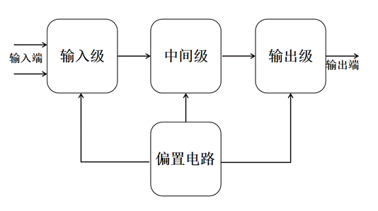

Operational amplifier (Integrated Operational Amplifier) is abbreviated as integrated operational amplifier, which is a multi-stage direct coupling amplifier circuit with high voltage gain, high input resistance and low output resistance.
Internal structure of op amp
The input stage is generally a differential amplifier circuit composed of BJT (bipolar transistor, current control device), JFET (junction field effect transistor, voltage control device) or MOSFET (oxide semiconductor field effect transistor), mainly using symmetrical The characteristic improves the common-mode rejection ratio. Its two input terminals constitute the inverting input terminal and the non-inverting input terminal of the entire circuit; the main function of the voltage amplifier stage is to increase the voltage gain, and it can be composed of YJ or multi-stage amplifier circuits; output stage It is generally composed of a voltage follower or a complementary voltage follower to reduce the output resistance and improve the load capacity; the bias circuit is to provide suitable working current for all levels. In addition, there are some auxiliary links. Such as level shift circuit, overload protection circuit and high frequency compensation circuit.
Op Amp Classification
01
According to the working principle
① Voltage amplification type
Realize voltage amplification, and the output circuit is equivalent to a voltage controlled voltage source.
② Current amplification type
Realize current amplification, and the output loop is equivalent to a current source controlled by current.
③ Transconductance amplification type
The input voltage is converted into output current, and the output loop is equivalent to a voltage-controlled current source.
④ Mutual resistance amplifier type
The input current is converted into output voltage, and the output loop is equivalent to a current-controlled voltage source.
02
By performance
① High resistance type
The characteristic is that the differential mode input impedance is very high, the input bias current is very small, generally rid>(109~1012)W, IIB is several to dozens of PA. It is suitable for measuring amplifying circuit, signal generating circuit, sampling-holding circuit.
② High-speed type
It is characterized by unity gain bandwidth and high conversion rate SR. Suitable for A/D, D/A converters, phase-locked loop circuits, and video amplifier circuits.
③ High JD type
It is characterized by low offset voltage, low temperature drift, low noise, and high gain. Suitable for precise measurement of weak signals, such as high-precision instruments.
④ Low power consumption type
It is characterized by low static power consumption and low operating voltage. It is suitable for remote sensing and remote measurement of portable instruments, space technology, industry and military.
⑤ General purpose
The characteristic is that the price is low, and the performance index requirements are generally met. Suitable for low frequency signals, simple signal processing.
Op amp parameter index
01
DC indicator
① Input offset voltage VIO and temperature drift αVIO
When the voltage at the output terminal of the integrated operational amplifier is zero, the compensation voltage applied between the two input terminals. The better the symmetry of the internal circuit, the smaller the input offset voltage, and the better the performance of the op amp; αVIO temperature drift is the ratio of the change in input offset voltage to the temperature change. Generally, the temperature drift of the op amp is between -10~20μV/℃. The temperature drift of precision op amp is less than 1μV/℃.
② Input bias current IIB
When the output DC voltage of the op amp is zero, the average value of the bias current of its two input terminals, usually the smaller the IIB, the smaller the IIO. Related to the manufacturing process, bipolar transistors are generally 80 to 500 nA, and field effect transistors are generally 1 nA.
③ Input offset current IIO and temperature drift dVIO
When the output DC voltage of the op amp is zero, the difference between the bias currents of its two input terminals. The better the symmetry of the internal circuit, the smaller the input offset current. Bipolar transistors are generally 20~200nA, and field effect transistors are generally less than 1nA; input offset current temperature drift (TCIOS) This parameter represents the input offset current generated when the temperature changes The amount of change. TCIOS is usually expressed in units of pA/?C.
④ Open loop differential mode gain Aod
The amplification factor of the integrated op amp without external feedback is called the open-loop differential mode gain, and the decibel number is 20 lg| Aod | The general op amp value is 80~120dB.
⑤ Common mode rejection ratio KCMR
When the operational amplifier works in the linear region, the ratio of the differential mode gain to the common mode gain is 20 lg KCMR.
⑥ Power supply rejection ratio
The ratio of the input offset voltage of the op amp to the change of the power supply voltage when the op amp is working in the linear region.
⑦ ZD common mode input voltage UIcmax
The ZD common mode signal that is allowed to input under the condition of normal amplification of the differential mode signal is generally defined as when the common mode rejection ratio drops by 6dB? The corresponding common mode input voltage is used as the ZD common mode input voltage.
⑧ ZD differential mode input voltage UIdmax
The two input terminals of the op amp are allowed to add ZD input voltage. When the allowable input voltage difference between the two input terminals of the op amp exceeds the ZD differential mode input voltage, the internal PN junction will break down and cause damage to the input stage of the op amp.
02
Communication indicators?
① Open loop bandwidth fH
The open-loop bandwidth fH is the signal frequency that reduces the DC open-loop differential mode gain Aod by 3dB (0.707 of the DC gain). The actual value is GBW=Gain*f.
②Unity gain bandwidth fc
Indicates the frequency at which the differential mode voltage amplification factor Aod drops to 0dB (DC open-loop differential mode gain Aod=1). Generally around 1MHz.
③ Conversion rate (also known as slew rate) SR
SR is the ZD value of the change in output voltage per unit time under the action of a large signal, and also indicates the ability of the operational amplifier to adapt to sudden changes in signals. The larger the signal amplitude and the higher the frequency, the larger the slew rate SR. The actual value is 2*π*f*Vin*Gain.
④ Common mode input impedance
This parameter represents the ratio of the input common-mode voltage range to the variation of the bias current in this range when the operational amplifier is working in the linear region. At low frequencies, it appears as a common-mode resistance, with a typical value above 108 ohms.
⑤ Differential mode input impedance (also called input impedance) rid
This parameter represents the ratio of the change of the input voltage to the corresponding change of the input current. The change of the voltage causes the change of the current. The greater the differential mode input impedance, the smaller the signal demand current.
⑥ Output impedance
This parameter refers to the internal equivalent small signal impedance of the output terminal when the operational amplifier is working in the linear region.
⑦ Full power bandwidth BW
In the rated load, the closed-loop gain of the op amp is 1 times (DC open-loop differential mode gain Aod = 1), and a constant amplitude sinusoidal signal is input to the input terminal of the op amp, so that the amplitude of the op amp is ZD. Frequency of. Full power bandwidth = conversion rate/2πVop (Vop is the peak output amplitude of the op amp).
⑧ Static power consumption
Indicates the power consumption of the op amp under no signal condition. When the power supply voltage is 15V, the static power consumption of the bipolar transistor is generally 50-100mW, and the field effect transistor is generally 1mW.
⑨ Establishment time
In the rated load, the closed-loop gain of the op amp is 1 times (DC open-loop differential mode gain Aod = 1), a step large signal is input to the input end of the op amp to increase the output of the op amp from 0 to The time required for a given value.
⑩ Input voltage noise density (eN), input current noise density (iN)
Noise component.
Op-amp calculation ideas
Virtual short and virtual break are the basic points of analyzing op amps. (Introduction of negative feedback)
01
Short
Virtual short refers to that under ideal circumstances, the potentials of the two input terminals are equal, as if the two input terminals are shorted together, but in fact they are not shorted, which is called “virtual short”. The necessary condition for virtual short is that the op amp introduces deep negative feedback. In the linear application of the integrated operational amplifier, it can be approximately considered that when uN-uP=0, uN=uP, that is, the inverting and non-inverting input terminals are equivalent to a short circuit, so it is called a false short circuit, or “virtual short” for short.
02
False
Virtual cut-off means that under ideal conditions, the current flowing into the input of the integrated operational amplifier is zero. This is because the input resistance of an ideal op amp is infinite, just like an open circuit between the two input terminals of the op amp. But in fact, there is no open circuit, which is called “virtual disconnection”. When the input current of the two input terminals is zero, that is, iN=iP=0, it can be considered that the inverting and non-inverting input terminals are equivalent to a disconnection, which is called false disconnection, or “virtual disconnection” for short.
Op Amp Protection Measures
The safety protection of the integrated operational amplifier has three aspects: power supply protection, input protection and output protection.
01
Power protection
The common faults of the power supply are the polarity connection of the power supply and the voltage jump. Power reverse connection protection and power supply voltage mutation protection.


02
Input protection
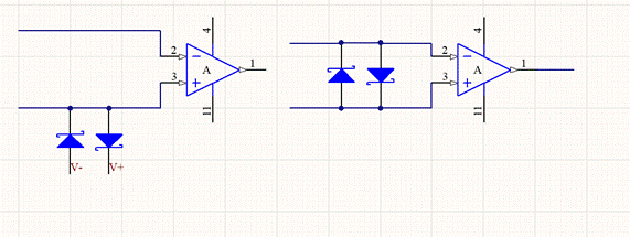
If the input differential mode voltage of the integrated operational amplifier is too high or the input common mode voltage is too high (beyond the limit parameter range of the integrated operational amplifier), the integrated operational amplifier will also be damaged.


03
Output protection
When the integrated operational amplifier is overloaded or the output terminal is short-circuited, if there is no protection circuit, the operational amplifier will be damaged. Some integrated op amps have built-in current-limiting protection or short-circuit protection.

Six Military Rules for Operational Amplifiers
As a general analog device of Z, operational amplifiers are widely used in signal conversion and conditioning, ADC sampling front-end, power supply circuits and other occasions. Although the peripheral circuit of the op amp is simple, there are still many points that need to be paid attention to during use.
01
Pay attention to whether the input voltage exceeds the limit
Take the ADI device as an example, the input electrical characteristics in the ADI data sheet can be seen under the condition of the power supply voltage of 15V, the input voltage range is 13.5V, if the input voltage exceeds the range, then the op amp will not work properly , There are some unexpected situations. There are some op amps that are labeled not the input voltage range, but the common-mode input voltage range. For example, TI’s TLC2272 has a common-mode input range of 0-3.5V under the condition of a single power supply of 5V. In fact, the common-mode input range is 0-3.5V when the op amp works normally. The input voltage of the terminal and the inverting terminal is basically the same (virtual short and virtual break), so “input voltage range” and “common mode input voltage range” have the same meaning.
02
Do not connect Capacitors directly to the output of the op amp
In the DC signal amplifying circuit, sometimes in order to reduce the noise, the decoupling capacitor is directly connected to the output of the op amp. Although the DC signal is amplified, it is very unsafe to do so. When there is a step signal input or at the moment of power-on, the output current of the op amp will be relatively large, and the capacitor will change the phase characteristics of the loop, causing the circuit to self-oscillate, which we do not want to see.
The correct decoupling capacitor should form an RC circuit, that is, a Resistor is connected in series at the output of the op amp, and then the decoupling capacitor is connected in parallel. Doing so can greatly reduce the instantaneous output current of the op amp, and will not affect the phase characteristics of the loop, which can avoid oscillation.
03
Do not connect capacitors in parallel in the feedback loop of the amplifying circuit
It is also a circuit for DC signal amplification. In order to decoupling, the capacitor is accidentally connected to the feedback loop, and the phase of the feedback signal changes, and it is easy to oscillate. Therefore, in the amplifying circuit, the feedback loop cannot add any circuit that affects the phase of the signal. This extends to the regulated power supply circuit, and the capacitor connected to the feedback pin is wrong. In order to reduce the ripple, the capacitor can be connected in parallel with the feedback resistor to appropriately increase the negative feedback effect of the ripple and suppress the output ripple.
04
Pay attention to the output swing of the op amp
No op amp can be an ideal op amp, and the output voltage cannot reach the power supply voltage. Generally, MOS-based op amps are rail-to-rail op amps. Under no-load conditions, the output can reach the power supply voltage, but the output will take a certain amount. The greater the load, the more the output will drop.
05
Pay attention to the layout of the feedback loop
The components of the feedback loop must be close to the op amp, and the PCB traces should be as short as possible, and at the same time, avoid interference sources such as digital signals and crystal oscillators. If the layout of the feedback loop is unreasonable, it will easily introduce noise, which will seriously cause self-oscillation.
06
Pay attention to power supply filtering
The power supply filtering of the op amp cannot be ignored, and the quality of the power supply directly affects the output. Especially for high-speed op amps, the power supply ripple has a great interference to the output of the op amp, and it will become self-oscillation if it is not correct. Therefore, a good op amp filter is to add a 0.1uF decoupling capacitor and a tens of uF tantalum capacitor next to the power pin of the op amp, or connect a small Inductor or magnetic bead in series, the effect will be better.
The input stage is generally a differential amplifier circuit composed of BJT (bipolar transistor, current control device), JFET (junction field effect transistor, voltage control device) or MOSFET (oxide semiconductor field effect transistor), mainly using symmetrical The characteristic improves the common-mode rejection ratio. Its two input terminals constitute the inverting input terminal and the non-inverting input terminal of the entire circuit; the main function of the voltage amplifier stage is to increase the voltage gain, and it can be composed of YJ or multi-stage amplifier circuits; output stage It is generally composed of a voltage follower or a complementary voltage follower to reduce the output resistance and improve the load capacity; the bias circuit is to provide suitable working current for all levels. In addition, there are some auxiliary links. Such as level shift circuit, overload protection circuit and high frequency compensation circuit.

Operational amplifier (Integrated Operational Amplifier) is abbreviated as integrated operational amplifier, which is a multi-stage direct coupling amplifier circuit with high voltage gain, high input resistance and low output resistance.
Internal structure of op amp
The input stage is generally a differential amplifier circuit composed of BJT (bipolar transistor, current control device), JFET (junction field effect transistor, voltage control device) or MOSFET (oxide semiconductor field effect transistor), mainly using symmetrical The characteristic improves the common-mode rejection ratio. Its two input terminals constitute the inverting input terminal and the non-inverting input terminal of the entire circuit; the main function of the voltage amplifier stage is to increase the voltage gain, and it can be composed of YJ or multi-stage amplifier circuits; output stage It is generally composed of a voltage follower or a complementary voltage follower to reduce the output resistance and improve the load capacity; the bias circuit is to provide suitable working current for all levels. In addition, there are some auxiliary links. Such as level shift circuit, overload protection circuit and high frequency compensation circuit.
Op Amp Classification
01
According to the working principle
① Voltage amplification type
To achieve voltage amplification, the output loop is equivalent to a voltage controlled voltage source.
② Current amplification type
Realize current amplification, and the output loop is equivalent to a current source controlled by current.
③ Transconductance amplification type
The input voltage is converted into output current, and the output loop is equivalent to a voltage-controlled current source.
④ Mutual resistance amplifier type
The input current is converted into output voltage, and the output loop is equivalent to a current-controlled voltage source.
02
By performance
① High resistance type
The characteristic is that the differential mode input impedance is very high, the input bias current is very small, generally rid>(109~1012)W, IIB is several to dozens of PA. It is suitable for measuring amplifying circuit, signal generating circuit, sampling-holding circuit.
② High-speed type
It is characterized by unity gain bandwidth and high conversion rate SR. Suitable for A/D, D/A converters, phase-locked loop circuits, and video amplifier circuits.
③ High JD type
It is characterized by low offset voltage, low temperature drift, low noise, and high gain. Suitable for precision measurement of weak signals, such as high-precision instruments.
④ Low power consumption type
It is characterized by low static power consumption and low operating voltage. It is suitable for remote sensing and remote measurement of portable instruments, space technology, industry and military.
⑤ General purpose
It is characterized by low price and generally meets the performance index requirements. Suitable for low frequency signals, simple signal processing.
Op amp parameter index
01
DC indicator
① Input offset voltage VIO and temperature drift αVIO
When the voltage at the output terminal of the integrated operational amplifier is zero, the compensation voltage applied between the two input terminals. The better the symmetry of the internal circuit, the smaller the input offset voltage, and the better the performance of the op amp; αVIO temperature drift is the ratio of the change in input offset voltage to the temperature change. Generally, the temperature drift of the op amp is between -10~20μV/℃. The temperature drift of precision op amp is less than 1μV/℃.
② Input bias current IIB
When the output DC voltage of the op amp is zero, the average value of the bias current of its two input terminals, usually the smaller the IIB, the smaller the IIO. Related to the manufacturing process, bipolar transistors are generally 80 to 500 nA, and field effect transistors are generally 1 nA.
③ Input offset current IIO and temperature drift dVIO
When the output DC voltage of the op amp is zero, the difference between the bias currents of its two input terminals. The better the symmetry of the internal circuit, the smaller the input offset current. Bipolar transistors are generally 20~200nA, and field effect transistors are generally less than 1nA; input offset current temperature drift (TCIOS) This parameter represents the input offset current generated when the temperature changes The amount of change. TCIOS is usually expressed in units of pA/?C.
④ Open loop differential mode gain Aod
The amplification factor of the integrated op amp without external feedback is called the open-loop differential mode gain, and the decibel number is 20 lg| Aod | The general op amp value is 80~120dB.
⑤ Common mode rejection ratio KCMR
When the operational amplifier works in the linear region, the ratio of the differential mode gain to the common mode gain is 20 lg KCMR.
⑥ Power supply rejection ratio
The ratio of the input offset voltage of the op amp to the change of the power supply voltage when the op amp is working in the linear region.
⑦ ZD common mode input voltage UIcmax
The ZD common mode signal that is allowed to input under the condition of normal amplification of the differential mode signal is generally defined as when the common mode rejection ratio drops by 6dB? The corresponding common mode input voltage is used as the ZD common mode input voltage.
⑧ ZD differential mode input voltage UIdmax
The two input terminals of the op amp are allowed to add ZD input voltage. When the allowable input voltage difference between the two input terminals of the op amp exceeds the ZD differential mode input voltage, the internal PN junction will break down and cause damage to the input stage of the op amp.
02
Communication indicators?
① Open loop bandwidth fH
The open-loop bandwidth fH is the signal frequency that reduces the DC open-loop differential mode gain Aod by 3dB (0.707 of the DC gain). The actual value is GBW=Gain*f.
②Unity gain bandwidth fc
Indicates the frequency at which the differential mode voltage amplification factor Aod drops to 0dB (DC open-loop differential mode gain Aod=1). Generally around 1MHz.
③ Conversion rate (also known as slew rate) SR
SR is the ZD value of the change in output voltage per unit time under the action of a large signal, and also indicates the ability of the operational amplifier to adapt to sudden changes in signals. The larger the signal amplitude and the higher the frequency, the larger the slew rate SR. The actual value is 2*π*f*Vin*Gain.
④ Common mode input impedance
This parameter represents the ratio of the input common-mode voltage range to the variation of the bias current in this range when the operational amplifier is working in the linear region. At low frequencies, it appears as a common-mode resistance, with a typical value above 108 ohms.
⑤ Differential mode input impedance (also called input impedance) rid
This parameter represents the ratio of the change of the input voltage to the corresponding change of the input current. The change of the voltage causes the change of the current. The greater the differential mode input impedance, the smaller the signal demand current.
⑥ Output impedance
This parameter refers to the internal equivalent small signal impedance of the output terminal when the operational amplifier is working in the linear region.
⑦ Full power bandwidth BW
In the rated load, the closed-loop gain of the op amp is 1 times (DC open-loop differential mode gain Aod = 1), and a constant amplitude sinusoidal signal is input to the input terminal of the op amp, so that the amplitude of the op amp is ZD. Frequency of. Full power bandwidth = conversion rate/2πVop (Vop is the peak output amplitude of the op amp).
⑧ Static power consumption
Indicates the power consumption of the op amp under no signal condition. When the power supply voltage is 15V, the static power consumption of the bipolar transistor is generally 50-100mW, and the field effect transistor is generally 1mW.
⑨ Establishment time
In the rated load, the closed-loop gain of the op amp is 1 times (DC open-loop differential mode gain Aod = 1), a step large signal is input to the input end of the op amp to increase the output of the op amp from 0 to The time required for a given value.
⑩ Input voltage noise density (eN), input current noise density (iN)
Noise component.
Op-amp calculation ideas
Virtual short and virtual break are the basic points of analyzing op amps. (Introduction of negative feedback)
01
Short
Virtual short refers to that under ideal conditions, the potentials of the two input terminals are equal, as if the two input terminals are shorted together, but in fact they are not shorted, which is called “virtual short”. The necessary condition for virtual short is that the op amp introduces deep negative feedback. In the linear application of the integrated operational amplifier, it can be approximately considered that when uN-uP=0, uN=uP, that is, the inverting and non-inverting input terminals are equivalent to a short circuit, so it is called a false short circuit, or “virtual short” for short.
02
False
Virtual cut-off means that under ideal conditions, the current flowing into the input of the integrated operational amplifier is zero. This is because the input resistance of an ideal op amp is infinite, just like an open circuit between the two input terminals of the op amp. But in fact, there is no open circuit, which is called “virtual disconnection”. When the input current of the two input terminals is zero, that is, iN=iP=0, it can be considered that the inverting and non-inverting input terminals are equivalent to a disconnection, which is called false disconnection, or “virtual disconnection” for short.
Op Amp Protection Measures
The safety protection of the integrated operational amplifier has three aspects: power supply protection, input protection and output protection.
01
Power protection
The common faults of the power supply are the polarity connection of the power supply and the voltage jump. Power reverse connection protection and power supply voltage mutation protection.
02
Input protection
If the input differential mode voltage of the integrated operational amplifier is too high or the input common mode voltage is too high (beyond the limit parameter range of the integrated operational amplifier), the integrated operational amplifier will also be damaged.
03
Output protection
When the integrated operational amplifier is overloaded or the output terminal is short-circuited, if there is no protection circuit, the operational amplifier will be damaged. Some integrated op amps have built-in current-limiting protection or short-circuit protection.

Six Military Rules for Operational Amplifiers
As a general analog device of Z, operational amplifiers are widely used in signal conversion and conditioning, ADC sampling front-end, power supply circuits and other occasions. Although the peripheral circuit of the op amp is simple, there are still many points that need to be paid attention to during use.
01
Pay attention to whether the input voltage exceeds the limit
Take the ADI device as an example, the input electrical characteristics in the ADI data sheet can be seen under the condition of the power supply voltage of 15V, the input voltage range is 13.5V, if the input voltage exceeds the range, then the op amp will not work properly , There are some unexpected situations. There are some op amps that are labeled not the input voltage range, but the common-mode input voltage range. For example, TI’s TLC2272 has a common-mode input range of 0-3.5V under the condition of a single power supply of 5V. In fact, the common-mode input range is 0-3.5V when the op amp works normally. The input voltage of the terminal and the inverting terminal is basically the same (virtual short and virtual break), so “input voltage range” and “common mode input voltage range” have the same meaning.
02
Do not connect capacitors directly to the output of the op amp
In the DC signal amplifying circuit, sometimes in order to reduce the noise, the decoupling capacitor is directly connected to the output of the op amp. Although the DC signal is amplified, it is very unsafe to do so. When there is a step signal input or at the moment of power-on, the output current of the op amp will be relatively large, and the capacitor will change the phase characteristics of the loop, causing the circuit to self-oscillate, which we do not want to see.
The correct decoupling capacitor should form an RC circuit, that is, a resistor is connected in series at the output of the op amp, and then the decoupling capacitor is connected in parallel. Doing so can greatly reduce the instantaneous output current of the op amp, and will not affect the phase characteristics of the loop, which can avoid oscillation.
03
Do not connect capacitors in parallel in the feedback loop of the amplifying circuit
It is also a circuit for DC signal amplification. For decoupling, the capacitor is accidentally connected to the feedback loop, and the phase of the feedback signal changes, and it is easy to oscillate. Therefore, in the amplifying circuit, the feedback loop cannot add any circuit that affects the phase of the signal. This extends to the regulated power supply circuit, and the capacitor connected to the feedback pin is wrong. In order to reduce the ripple, the capacitor can be connected in parallel with the feedback resistor to appropriately increase the negative feedback effect of the ripple and suppress the output ripple.
04
Pay attention to the output swing of the op amp
No op amp can be an ideal op amp, and the output voltage cannot reach the power supply voltage. Generally, MOS-based op amps are rail-to-rail op amps. Under no-load conditions, the output can reach the power supply voltage, but the output will have a certain amount The greater the load, the more the output will drop.
05
Pay attention to the layout of the feedback loop
The components of the feedback loop must be close to the op amp, and the PCB traces must be as short as possible, and at the same time, avoid interference sources such as digital signals and crystal oscillators. If the layout of the feedback loop is unreasonable, it will easily introduce noise, which will seriously cause self-oscillation.
06
Pay attention to power supply filtering
The power supply filtering of the op amp cannot be ignored, and the quality of the power supply directly affects the output. Especially for high-speed op amps, the power supply ripple has a great interference to the output of the op amp, and it will become self-oscillation if it is not correct. Therefore, a good op amp filter is to add a 0.1uF decoupling capacitor and a tens of uF tantalum capacitor next to the power pin of the op amp, or connect a small inductor or magnetic bead in series, the effect will be better.