Panasonic develops new Semiconductor substrate material

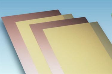
Panasonic has announced that its Industrial Solutions Company has commercialised a semiconductor package substrate material (Product No. R-1515V) that enables both low package warpage and high reliability.
The material has very low thermal expansion properties that reduce warping of the substrate during the packaging process and optimised mechanical properties that have been designed to lower the residual stress on solder joints created during reflow assembly. Mass production of the material is scheduled to start in July 2021.
According to Panasonic, current generation of advanced package designs exhibit a relatively large footprint, a plethora of I/Os and high-density interconnecting structures like those found in 2.5D packages and along with the operating performance improvements, most industrial and commercial applications will demand high assembly-level reliability from assembled packages.
Panasonic has developed a broad range of products for motherboard material and semiconductor packaging and assembly, including package substrates; encapsulation materials; and assembly-level reinforcement materials and by leveraging that expertise it has formulated a new semiconductor substrate material offering both low warpage and high assembly-level reliability.
Improving chip packaging reliability has required a reduction in the substrate warpage during packaging, that is, mounting chips on the IC substrate followed by an encapsulation process. In addition, the stress imparted to the solder balls during the reflow assembly process – during which the semiconductor package is assembled onto a motherboard – has also needed to be lowered to ensure long-term operational reliability.
According to Panasonic the coefficient of thermal expansion (CTE) of this new substrate material is much closer to that of silicon IC chips (4 ppm as measured by the company) reducing warpage caused by the thermal excursions experienced during packaging processes. In addition, the new substrate material features much improved thickness tolerances, ensuring stable junctions between the substrate and the IC chips, further improving the reliability of packaged chip. The modified flexibility and buffering properties of the new material alleviate the stress on solder balls, improving the assembly-level reliability.