“At present, in the early fire monitoring and alarm of buildings, the wired network is still used. The lines are scattered throughout the building and the initial installation cost is high. At the same time, the line itself is also a great fire hazard. Therefore, a new type of wireless fire monitoring system came into being, which is convenient and quick to install, and its cost is lower, and it has a larger application space. The microcontroller is one of the core components of the fire monitoring system. General-purpose microprocessors and microcontrollers cannot meet the low power consumption and low cost requirements of the node master chip in the wireless fire monitoring system.
“
At present, in the early fire monitoring and alarm of buildings, the wired network is still used. The lines are scattered throughout the building and the initial installation cost is high. At the same time, the line itself is also a great fire hazard. Therefore, a new type of wireless fire monitoring system came into being, which is convenient and quick to install, and its cost is lower, and it has a larger application space. The microcontroller is one of the core components of the fire monitoring system. General-purpose microprocessors and microcontrollers cannot meet the low power consumption and low cost requirements of the node master chip in the wireless fire monitoring system.
In order to master the core technology of the wireless fire monitoring system, establish a software and hardware platform with independent intellectual property rights, and promote the development of my country’s wireless fire monitoring system, it is necessary to develop a microprocessor for the wireless fire monitoring system. This article has completed the physical design of a microcontroller chip dedicated to the fire detection system.
1 SW-A chip architecture
SW-A chip is a dedicated digital-analog hybrid controller chip for wireless fire detection system based on ARM Cortex-M0. The bus adopts AMBA AHB and APB dual-bus architecture. The operating frequency can reach up to 50 MHz and supports multiple levels. Internal frequency division, it can also run at a very low frequency in standby mode; built-in a high sampling rate 12-bit successive approximation 8-channel ADC, which can sequentially scan from 8 sensors (such as temperature sensor, smoke sensor, light intensity sensor, etc.) ) The signal is directly sampled, converted, and saved. The main detection program can read the sampled data corresponding to the target sensor for processing and determine whether a fire has occurred.
Built-in 18 KBSRAM, which can be used as FLASH and RAM flexibly to meet fire monitoring and storage of simple processing procedures. It supports ISP (in-system programming) operation and IAP (in-application programming) operation, which is not only convenient for updating and upgrading the main fire monitoring program, but also for software optimization. The interface includes industry standard UART interface, SSI communication interface (supporting SPI, MicroWire and SSI protocol), and 3 groups (6 channels) PWM. The rich interfaces and functional modules make this chip have great potential in function expansion.
2 Physical design of SW-A chip
2.1 The physical design process adopted
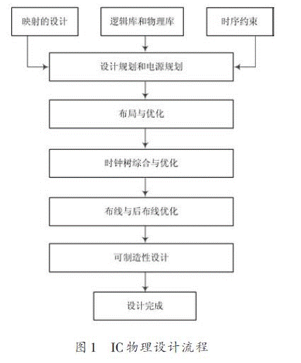
The physical design of the SW-A chip is carried out with the help of Synopsys’ EDA tool IC Compiler, using IC Compiler’s typical design process. Based on TSMC (TSMC) 180 nm CMOS process. After the physical design is ready (designing the logic library, setting the physical library, setting the TLU-Plus related files, and setting the read gate-level netlist and standard delay constraints), you can start the physical design, and complete the design planning (Designplanning), Placement, Clock tree Syn-thesis, Routing, and Chip Finish.

2.2 Design planning
Design Planning is a very important step in the physical design of the chip; it mainly includes Floorplan and Powerplant.
Under normal circumstances, before the layout starts, designers often need to spend a lot of time on floorplan and powerplan. The quality of the design plan directly determines the power consumption of the chip, the congestion of standard cells, Timing closure, power supply stability, etc. Therefore, design planning is the step with the most repetitions and manual design in the entire physical design process.
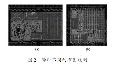
Floorplan must complete the IO layout, PAD placement, Macro (including analog modules, storage units, etc.) positioning, as well as the chip shape, congestion (Congestion) and area settings. As a user-oriented control chip, the layout of IO must comprehensively consider user needs and design requirements, and the vertical and horizontal dimensions of different functional PADs are also different. In this paper, the PAD with larger dimensions in both vertical and horizontal directions is placed on the north and south sides of the chip, and the PAD with a smaller unidirectional size is placed on the east and west sides of the chip with the large side facing south and north (see Figure 2(a)). Place the PAD around the chip with a larger size in both directions (see Figure 2(b)). This design is very effective in reducing the area of the chip.

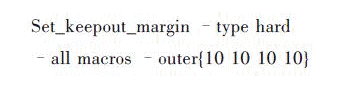
The Macros that the chip needs to be positioned include SRAM, ROM, ADC, and ANALOG_TOP. This article comprehensively considers their positional relationship with IO and locates them around the chip, so that a blank area can be reserved in the chip to place standard cells. In order to ensure the interconnection between the Macro and PAD and standard units, there is only a blank area around each Macro. Standard units are not allowed to be placed in this area under any circumstances. The specific commands are as follows:


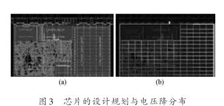
This chip is designed with a 40 μm reserved area between the core area of the standard cell and the Macro and the PAD for placing the power ring (PowerRing) and interconnecting wiring. In order to prevent the standard cells from overlapping, use the command to ensure that the standard cells can only be placed in channels with a height greater than 10 μm. After setting the chip layout plan, use the command creat_fp_placement for pre-layout. This chip is designed and produced using TSMC 180 nm process. It requires a working voltage of 1.8 V and a tolerable maximum voltage fluctuation of ±10%. Therefore, when planning the power supply in this article, the power supply requirements of the chip and the voltage drop caused by the interconnection line are comprehensively considered ( IR-Drop) and a smaller power network area, two power rings and 14 power straps (Strap) are designed. After analyzing the power network (Analyze Pow-er Network), the maximum IR-Drop of this design is 29.7 mV. Figure 3(a) is the design plan of the chip, and Figure 3(b) is the voltage drop distribution diagram of the chip.


2.3 Layout
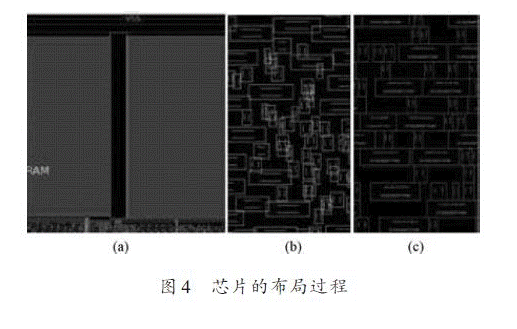
The quality of the placement is the key to the success or failure of the physical design of the chip. The main task of the layout is to complete the setup time of placing and repairing the standard units in the design. Before the layout officially starts, you need to use the check_physical_design command to check whether the layout preparation is complete. It must be ensured that the positions of all Hard Macro and IO are fixed; all logical pins and physical pins in the design correspond to each other; all logical units correspond to them The physical unit; the dimensions of all units in the design have been fixed. In order to facilitate the interconnection and routing, before starting to place the standard cells, a specific area in the chip can be set as a Place-ment Blockage (Place-ment Blockage). ICC tools have various restrictions, such as prohibiting standard cells for rough layout, only allowing standard cells for layout optimization, and only allowing wiring, etc.; in this design, multiple layout restriction areas are set to facilitate ADC, ANALOG_TOP, etc. Connection with IO (see Figure 4(a)).
After the layout is ready, you can use the place_opt command to perform layout with additional constraints. The command executes coarse place, high-fanout net synthesis, physical optimization, and legalization. Determine the location of the unit by the first three steps (see Figure 4(b)), and finally place the standard unit in the calculated position correctly through legalization (see Figure 4(c)). The specific commands for the physical design of this article are as follows:


Tools are required to repair areas other than the critical clock path, with a high degree of effort. Use the option “-congestion” control tool to reduce the congestion of the chip as much as possible to facilitate subsequent wiring, and use the option “-pow-er” to control tool optimization Leakage power consumption, dynamic power consumption and low-power layout.
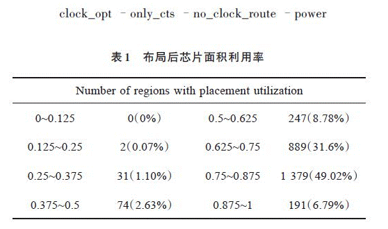
After the layout is completed, the area utilization of the chip is shown in Table 1. The congestion degree is concentrated between 0.625 and 0.875, and the congestion degree is moderate. There is neither waste of chip area due to low chip utilization nor excessive congestion. This leads to difficulties in subsequent design and even redesign.


2.4 Clock tree synthesis
One of the main tasks of Clock Tree Synthesis is to control the clock deviation within an acceptable range to ensure the efficient and error-free work of the chip. The clock tree synthesis strategy of this chip is as follows: the logic synthesis of the clock tree (clock-cts), the physical synthesis of the clock tree (clock-psyn) and the wiring of the clock tree (clock-route). The logic synthesis stage of the clock tree only completes two tasks: by calculating the delay on each clock path, the position and size of the buffer (buffer, inverter) that need to be inserted (controlled by the -only_cts command option) are obtained; due to the function of the clock network Consumption accounts for a very large proportion of total power consumption, so power consumption optimization (-power) must be performed during clock tree synthesis and no wiring is performed at this stage. The specific commands are as follows:


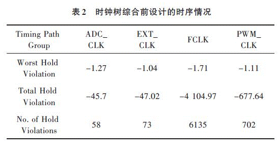
In the physical synthesis stage of the clock tree, the inserted buffer is placed in an accurate position, RC extraction is performed, and the maximum insertion delay, minimum insertion delay, maximum clock deviation, and maximum conversion time of the clock network are checked by referring to the delay constraint file (SDC). And repair the hold violation in the design. In order to facilitate the wiring of the non-clock network, the -ar-ea_recovery option needs to be added at this time to reduce the connection area. The power consumption is still optimized at this stage. When completing the clock tree routing, this article uses the arnoldi model to accurately calculate the delay of the clock tree and 15 cycles iterative method for clock routing. Table 2 is the timing situation of the design before clock synthesis. It is obvious that there are multiple critical paths and there are many establishment time violations; after the clock tree synthesis is completed, the clock check is performed, and no clock violation is found, indicating that the clock tree synthesis is completed.

2.5 Wiring and chip completion
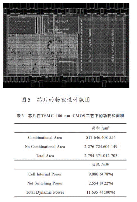
This article separates wiring and its optimization. First, complete global routing, detail rout-ing, and search&repair in the initial wiring stage, and then use topology algorithms to optimize the wiring, and at the same time The current leakage power consumption is optimized. In order to prevent the occurrence of the antenna effect, the antenna effect repair design is carried out on the chip during the chip completion stage. At this time, there are still blank areas in the chip, and the filer needs to be filled to meet the DRC requirements. Figure 5 is the physical design layout of the chip. Table 3 is the area and power consumption of the chip. It can be seen that the total area is 2 794 371.012 703 μm2, and the total power consumption is 11.635 4 mW. The simulation proves that the chip is operating at a clock frequency of 50 MHz Normal work, meet the design requirements, prove that this design is correct and effective.

3 Conclusion
Based on the TSMC 180 nm process, this paper has completed the physical design of a microprocessor chip used in the wireless fire monitoring system. After using different strategies to complete the chip layout planning, layout, clock tree synthesis, and wiring design steps, the results are obtained The layout, area, power consumption and other reports of the chip. After the physical design, the design indicators of the chip meet the design requirements, which proves the correctness of the physical design of the chip.
At present, in the early fire monitoring and alarm of buildings, the wired network is still used. The lines are scattered throughout the building and the initial installation cost is high. At the same time, the line itself is also a great fire hazard. Therefore, a new type of wireless fire monitoring system came into being, which is convenient and quick to install, and its cost is lower, and it has a larger application space. The microcontroller is one of the core components of the fire monitoring system. General-purpose microprocessors and microcontrollers cannot meet the low power consumption and low cost requirements of the node master chip in the wireless fire monitoring system.
In order to master the core technology of the wireless fire monitoring system, establish a software and hardware platform with independent intellectual property rights, and promote the development of my country’s wireless fire monitoring system, it is necessary to develop a microprocessor for the wireless fire monitoring system. This article has completed the physical design of a microcontroller chip dedicated to the fire detection system.
1 SW-A chip architecture
SW-A chip is a dedicated digital-analog hybrid controller chip for wireless fire detection system based on ARM Cortex-M0. The bus adopts AMBA AHB and APB dual-bus architecture. The operating frequency can reach up to 50 MHz and supports multiple levels. Internal frequency division, it can also run at a very low frequency in standby mode; built-in a high sampling rate 12-bit successive approximation 8-channel ADC, which can sequentially scan from 8 sensors (such as temperature sensor, smoke sensor, light intensity sensor, etc.) ) The signal is directly sampled, converted, and saved. The main detection program can read the sampled data corresponding to the target sensor for processing and determine whether a fire has occurred.
Built-in 18 KBSRAM, which can be used as FLASH and RAM flexibly to meet fire monitoring and storage of simple processing procedures. It supports ISP (in-system programming) operation and IAP (in-application programming) operation, which is not only convenient for updating and upgrading the main fire monitoring program, but also for software optimization. The interface includes industry standard UART interface, SSI communication interface (supporting SPI, MicroWire and SSI protocol), and 3 groups (6 channels) PWM. The rich interfaces and functional modules make this chip have great potential in function expansion.
2 Physical design of SW-A chip
2.1 The physical design process adopted
The physical design of the SW-A chip is carried out with the help of Synopsys’ EDA tool IC Compiler, using IC Compiler’s typical design process. Based on TSMC (TSMC) 180 nm CMOS process. After the physical design is ready (designing the logic library, setting the physical library, setting the TLU-Plus related files, and setting the read gate-level netlist and standard delay constraints), you can start the physical design, and complete the design planning (Designplanning), Placement, Clock tree Syn-thesis, Routing, and Chip Finish.

2.2 Design planning
Design Planning is a very important step in the physical design of the chip; it mainly includes Floorplan and Powerplant.
Under normal circumstances, before the layout starts, designers often need to spend a lot of time on floorplan and powerplan. The quality of the design plan directly determines the power consumption of the chip, the congestion of standard cells, Timing closure, power supply stability, etc. Therefore, design planning is the step with the most repetitions and manual design in the entire physical design process.
Floorplan must complete the IO layout, PAD placement, Macro (including analog modules, storage units, etc.) positioning, as well as the chip shape, congestion (Congestion) and area settings. As a user-oriented control chip, the layout of IO must comprehensively consider user needs and design requirements, and the vertical and horizontal dimensions of different functional PADs are also different. In this paper, the PAD with larger dimensions in both vertical and horizontal directions is placed on the north and south sides of the chip, and the PAD with a smaller unidirectional size is placed on the east and west sides of the chip with the large side facing south and north (see Figure 2(a)). Place the PAD around the chip with a larger size in both directions (see Figure 2(b)). This design is very effective in reducing the area of the chip.

The Macros that the chip needs to be positioned include SRAM, ROM, ADC, and ANALOG_TOP. This article comprehensively considers their positional relationship with IO and locates them around the chip, so that a blank area can be reserved in the chip to place standard cells. In order to ensure the interconnection between the Macro and PAD and standard units, there is only a blank area around each Macro. Standard units are not allowed to be placed in this area under any circumstances. The specific commands are as follows:
This chip is designed with a 40 μm reserved area between the core area of the standard cell and the Macro and the PAD for placing the power ring (PowerRing) and interconnecting wiring. In order to prevent the standard cells from overlapping, use the command to ensure that the standard cells can only be placed in channels with a height greater than 10 μm. After setting the chip layout plan, use the command creat_fp_placement for pre-layout. This chip is designed and produced using TSMC 180 nm process. It requires a working voltage of 1.8 V and a tolerable maximum voltage fluctuation of ±10%. Therefore, when planning the power supply in this article, the power supply requirements of the chip and the voltage drop caused by the interconnection line are comprehensively considered ( IR-Drop) and a smaller power network area, two power rings and 14 power straps (Strap) are designed. After analyzing the power network (Analyze Pow-er Network), the maximum IR-Drop of this design is 29.7 mV. Figure 3(a) is the design plan of the chip, and Figure 3(b) is the voltage drop distribution diagram of the chip.
2.3 Layout
The quality of the placement is the key to the success or failure of the physical design of the chip. The main task of the layout is to complete the setup time of placing and repairing the standard units in the design. Before the layout officially starts, you need to use the check_physical_design command to check whether the layout preparation is complete. It must be ensured that the positions of all Hard Macro and IO are fixed; all logical pins and physical pins in the design correspond to each other; all logical units correspond to them The physical unit; the dimensions of all units in the design have been fixed. In order to facilitate the interconnection and routing, before starting to place the standard cells, a specific area in the chip can be set as a Place-ment Blockage (Place-ment Blockage). ICC tools have various restrictions, such as prohibiting standard cells for rough layout, only allowing standard cells for layout optimization, and only allowing wiring, etc.; in this design, multiple layout restriction areas are set to facilitate ADC, ANALOG_TOP, etc. Connection with IO (see Figure 4(a)).
After the layout is ready, you can use the place_opt command to perform layout with additional constraints. The command executes coarse place, high-fanout net synthesis, physical optimization, and legalization. Determine the location of the unit by the first three steps (see Figure 4(b)), and finally place the standard unit in the calculated position correctly through legalization (see Figure 4(c)). The specific commands for the physical design of this article are as follows:
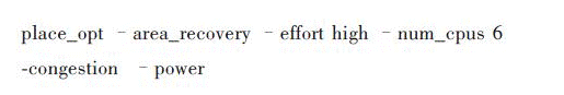
Tools are required to repair areas other than the critical clock path, with a high degree of effort. Use the option “-congestion” control tool to reduce the congestion of the chip as much as possible to facilitate subsequent wiring, and use the option “-pow-er” to control tool optimization Leakage power consumption, dynamic power consumption and low-power layout.
After the layout is completed, the area utilization of the chip is shown in Table 1. The congestion degree is concentrated between 0.625 and 0.875, and the congestion degree is moderate. There is neither waste of chip area due to low chip utilization nor excessive congestion. This leads to difficulties in subsequent design and even redesign.
2.4 Clock tree synthesis
One of the main tasks of Clock Tree Synthesis is to control the clock deviation within an acceptable range to ensure the efficient and error-free work of the chip. The clock tree synthesis strategy of this chip is as follows: the logic synthesis of the clock tree (clock-cts), the physical synthesis of the clock tree (clock-psyn) and the wiring of the clock tree (clock-route). The logic synthesis stage of the clock tree only completes two tasks: by calculating the delay on each clock path, the position and size of the buffer (buffer, inverter) that need to be inserted (controlled by the -only_cts command option) are obtained; due to the function of the clock network Consumption accounts for a very large proportion of total power consumption, so power consumption optimization (-power) must be performed during clock tree synthesis and no wiring is performed at this stage. The specific commands are as follows:
In the physical synthesis stage of the clock tree, the inserted buffer is placed in an accurate position, RC extraction is performed, and the maximum insertion delay, minimum insertion delay, maximum clock deviation, and maximum conversion time of the clock network are checked by referring to the delay constraint file (SDC). And repair the hold violation in the design. In order to facilitate the wiring of the non-clock network, the -ar-ea_recovery option needs to be added at this time to reduce the connection area. The power consumption is still optimized at this stage. When completing the clock tree routing, this article uses the arnoldi model to accurately calculate the delay of the clock tree and 15 cycles iterative method for clock routing. Table 2 shows the timing situation of the design before clock synthesis. It is obvious that there are multiple critical paths and there are many establishment time violations; after the clock tree synthesis is completed, the clock is checked again, and no clock violation is found, indicating that the clock tree synthesis is complete.

2.5 Wiring and chip completion
This article separates routing and optimization. First, complete global routing, detail rout-ing, and search & repair in the initial routing stage, and then use topology algorithms to optimize the routing, and at the same time The current leakage power consumption is optimized. In order to prevent the occurrence of the antenna effect, the antenna effect repair design is carried out on the chip during the chip completion stage. At this time, there are still blank areas in the chip, and the filer needs to be filled to meet the DRC requirements. Figure 5 is the physical design layout of the chip, and Table 3 is the area and power consumption of the chip. It can be seen that the total area is 2 794 371.012 703 μm2, and the total power consumption is 11.635 4 mW. The simulation proves that the chip is operating at a clock frequency of 50 MHz Normal work, meet the design requirements, prove that this design is correct and effective.

3 Conclusion
Based on the TSMC 180 nm process, this paper has completed the physical design of a microprocessor chip used in the wireless fire monitoring system. After using different strategies to complete the chip layout planning, layout, clock tree synthesis, and wiring design steps, the results are obtained The layout, area, power consumption and other reports of the chip. After the physical design, the design indicators of the chip meet the design requirements, which proves the correctness of the physical design of the chip.