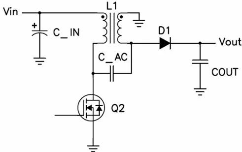
Figure 1 The SEPIC converter uses a switch to raise and lower the output voltage

The current and voltage waveforms of this circuit are similar to continuous current mode (CCM) reverse circuits. When Q1 is turned on, it uses the input voltage of the coupled inductor main stage to form energy in the circuit.
When Q1 is turned off, the inductor voltage reverses and is then clamped to the output voltage. The capacitor C_AC is the difference between the SEPIC and the reverse circuit; when Q1 is turned on, the secondary inductor current flows through it and then grounds. When Q1 is off, the primary inductor current flows through C_AC, thereby increasing the output current flowing through D1.
Compared with the reverse circuit, a big advantage of this topology is that the FET and diode voltages are both clamped by C_AC, and there is very little ringing in the circuit. In this way, we can choose to use a lower voltage, and thus produce a higher efficiency device.
Since this topology is similar to the reverse topology, many people would think that a set of tightly coupled windings is required. However, this is not the case. Figure 2 shows the two operating states of continuous SEPIC, the transformer has been modeled by leakage inductance (LL), magnetizing inductance (LM) and an ideal transformer (T).
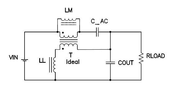
After inspection, the voltage of the leakage inductance is equal to the voltage of C_AC. Therefore, a small value of C_AC or a large AC voltage with a small leakage inductance will form a large loop current. Larger loop currents will reduce the efficiency and EMI performance of the converter, and this situation is undesirable. One way to reduce this large loop current is to increase the coupling capacitor (C_AC).
However, this comes at the cost of cost, size and reliability. A more astute method is to increase the leakage inductance, which can be easily achieved when a custom magnetic component is specified.
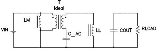
2a) mosfet is turned on: VLL = VC_AC -VIN = ∆VC_AC(DC part is deleted)

2b) MOSFET off: VLL = VIN + VOUT -VC_AC -VOUT = ∆VC_AC (DC part deleted)
Figure 2a and 2b SEPIC converter in two working states.

The AC voltage of the leakage inductance is equal to the coupling capacitor voltage.
Interestingly, very few manufacturers have realized this fact, and many manufacturers have produced low leakage inductance inductors for SEPIC applications.
On the other hand, Coilcraft has a 47 uH MSD1260 with a leakage inductance of about 0.5 uH. At the same time, it has also recently developed other versions of this design, which has a leakage inductance of more than 10 uH. It will be introduced in “, so stay tuned.