
The current transfer printing process has a number of limitations which have made it challenging to create more large-scale, complex flexible devices.
Precisely controlling critical variables like the speed of transfer, and the adhesion and orientation of the nanostructure, makes it difficult to ensure each stamp is identical to the last.
An incomplete or misaligned polymeric stamp onto the final substrate can lead to substandard electronic performance or even prevent devices from working.
While processes have been developed to make the stamping transfer more effective, they often require additional equipment like lasers and magnets, adding additional manufacturing cost.
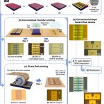
The Glasgow team have removed one stage of the conventional transfer printing process. Instead of transferring nanostructures to a soft polymeric stamp before it is transferred to the final substrate, their new process what they call ‘direct roll transfer’ to print silicon straight onto a flexible surface.
The process begins with the fabrication of a thin silicon nanostructure of less than 100 nanometres. Then the receiving substrate – a flexible, high-performance plastic foil material called polyimide – is covered in an ultrathin layer of chemicals to improve adhesion.
The prepared substrate is wrapped around a metal tube, and a computer-controlled machine developed by the team then rolls the tube over the silicon wafer, transferring it to the flexible material.
By carefully optimising the process, the team have managed to create highly-uniform prints over an area of about 10 square centimetres, with around 95% transfer yield – significantly higher than most conventional transfer printing processes at the nanometre scale.
The research was supported by funding from the Engineering and Physical Sciences Research Council (EPSRC)