Reducing supply-chain risk is typically a low priority when starting a new project. Device procurement often takes a back seat to goals such as the implementation of a new feature, improving circuit accuracy, precision, or increasing battery life.
But with some creativity and forward thinking, minimizing supply-chain risk is possible during device selection, and when working on schematics and layout before generating a final bill of materials (BOM). By selecting components in packages that work in a dual-footprint layout, you can add more flexibility to the supply chain and reduce risk by increasing the number of devices that can be used in a given circuit design.
Selecting a dual-footprint device
While this concept applies to many different types of devices and device packages, in this article I will explore the dual-footprint concept leveraging a low-dropout linear regulator (LDO) in small-outline Transistor (SOT-23) and extra-small outline no-lead (X2SON) packages. Because the X2SON is small enough to fit inside the SOT-23 footprint, you can double the number of components supported by the same printed circuit board (PCB) layout without increasing the design’s physical size.
Multiple other packages could work in a dual layout without taking up more board space. However, if there is plenty of space on the PCB, it is always possible to put the two footprints side-by-side rather than placing them on top of each other.
For this example, let’s assume that the system is powered from a 5-V source and needs to supply 3.3 V to a maximum load of 100 mA to maintain the lowest possible standby power. Let’s also assume you will use an external device, like a microcontroller, to disable the LDO with an enable (EN) pin. In order to design for supply chain flexibility, it is necessary to think about different ways to solve a specific design requirement with as many devices as possible. I will explore three different approaches that can be used to improve the supply chain flexibility of this design.
First, consider the different types of devices that could work in the system. If you select a fixed-output device, is there a device with a similar footprint that has an adjustable output? The TLV755P and TLV758P from Texas Instruments (TI), shown in Figure 1, are good examples of nearly pin-to-pin compatible fixed- and adjustable-output LDOs in a SOT-23 package.

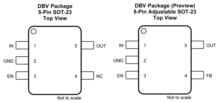
Figure 1: TLV755P (left) and TLV758P (right) pinouts (Source: Texas Instruments) Click for larger image.
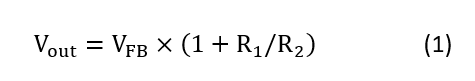
Pin No. 4 is not connected (NC) on the fixed-output TLV755P, but would be connected to a Resistor divider to set the output voltage on the TLV758P using Equation 1. By adding footprints for feedback resistors, the design can support two different integrated circuits (ICs) instead of only one.

Second, think about whether the selected device comes in multiple packages. For this example, let’s focus on reducing the amount of power consumption in the system during power on and shutdown by selecting TI’s 25-nA quiescent current TPS7A02 family of LDOs. The TPS7A02 data sheet confirms that the 1 × 1-mm X2SON package is small enough to fit between the pads of the SOT-23 package, and the pinout diagram shows that it is possible to orient the X2SON such that you can connect the VIN and VOUT of the SOT-23 and X2SON together in a way that will keep current flowing in the same direction regardless of which package you use in the final design.
Third, consider if there are any pin-to-pin compatible parts with similar performance that you could use as alternates. The TPS7A02 is pin-to-pin compatible with several other TI LDOs, such as the TPS7A03 and TPS7A05. By incorporating the dual-footprint practice and finding pin-to-pin alternates that meet the system requirements, your design can now support six different LDOs as opposed to one, helping reduce supply-chain risk.
Schematic and layout example
Similar to any schematic where you have do not install (DNI) resistors or capacitors to enable multiple circuit variants on the same PCB, the two ICs are drawn in parallel, as shown in Figure 2. Following the standard DNI practice, only one device is populated on the assembled PCB.
The data sheet recommends a nominal 1-µF ceramic input capacitor and a nominal 1-µF output capacitor with an effective minimum capacitance of 0.5 µF required for stability. On the SOT-23 package, you can leave the NC pin floating or tied to ground (GND). In this example, tying the NC pin to GND provides a more continuous top-side ground layer and has minimal cutouts between input capacitor GND, the IC GND and the output capacitor GND.

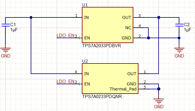
Figure 2: Dual-footprint schematic example (Source: Texas Instruments)
As shown in Figure 3, the X2SON package can fit between pin No. 1 and pin No. 5 (VIN and VOUT) of the SOT-23 package. Orienting the X2SON package such that the current flow from VIN to VOUT is the same in either variant adds virtually no area to the overall footprint because of the small 1 × 1-mm package size.

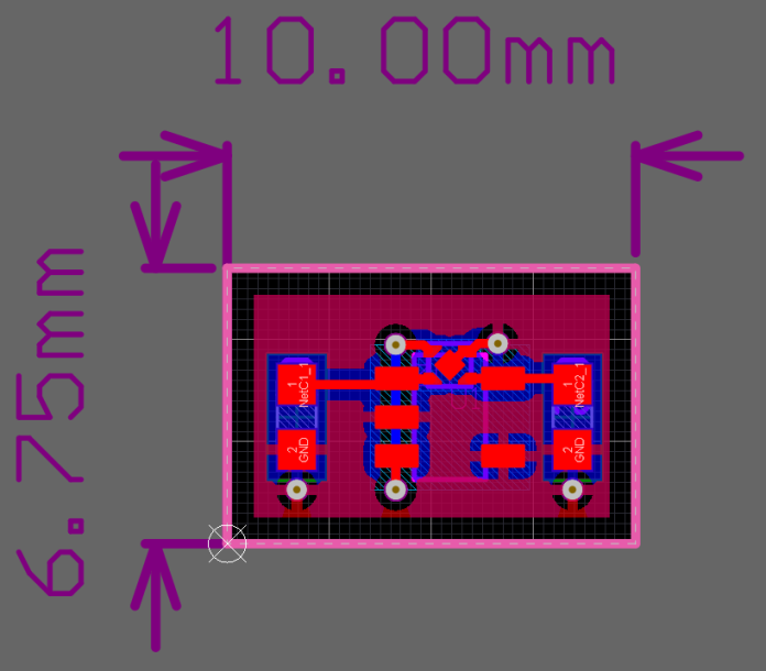
Figure 3: Layout example of dual-footprint TPS7A02 SOT-23 and X2SON packages (Source: Texas Instruments)
Figure 3 shows a two-layer board with multiple ground vias, but you can add a second output capacitor footprint to reduce the output current loop area in the X2SON case. You can break out the LDO_EN signal with a pair of vias and run one trace on the bottom layer to another source to control power sequencing if required. The total solution size area ends up being approximately 4 × 7 mm when using 0603 input and output capacitors, as shown in Figures 3 and 4.

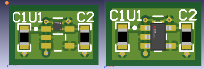
Figure 4: 3D model of a dual-footprint configuration with each package installed (Source: Texas Instruments)
Conclusion
By considering device package footprint size and pin-to-pin compatible alternatives, and having the flexibility to support multiple PCB build variants, it is possible to reduce supply-chain risk during the earliest stages of a design. While I focused specifically on LDO design flexibility, you can apply the same principles to many components, as long as you take a critical look at the package sizes and pinouts of the devices you’re selecting for a given design.
about Texas Instruments