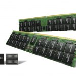
Samsung has begun mass producing 14nm DRAM using EUV technology.
Following the company’s shipment of its first EUV DRAM in March of last year, Samsung has increased the number of EUV layers to five to deliver today’s DDR5 devices.
As DRAM continues to scale down the 10nm-range, EUV technology becomes increasingly important to improve patterning accuracy for higher performance and greater yields.
By applying five EUV layers to its 14nm DRAM, Samsung has achieved the highest bit density while enhancing the overall wafer productivity by approximately 20%.
Additionally, the 14nm process can help bring down power consumption by nearly 20% compared to the previous-generation DRAM node.
Leveraging the latest DDR5 standard, Samsung’s 14nm DRAM will deliver speeds of up to 7.2 Gbps, which is more than twice the DDR4 speed of up to 3.2Gbps.
Samsung plans to expand its 14nm DDR5 portfolio to support data center, supercomputer and enterprise server applications. Also, Samsung expects to grow its 14nm DRAM chip density to 24Gb.