“The goal of this lab activity is to investigate an active rectifier circuit. Specifically, an active rectifier circuit integrates an operational amplifier, a low-threshold P-channel mosfet, and a feedback loop to synthesize a unidirectional current valve or rectifier with a lower forward voltage drop than a conventional PN junction diode.
“
By Doug Mercer, Consulting Researcher and Antoniu Miclaus, Systems Applications Engineer
Target
The goal of this lab activity is to investigate an active rectifier circuit. Specifically, an active rectifier circuit integrates an operational amplifier, a low-threshold P-channel MOSFET, and a feedback loop to synthesize a unidirectional current valve or rectifier with a lower forward voltage drop than a conventional PN junction diode.
background knowledge
When a power supply uses traditional diodes to rectify AC voltage to obtain DC voltage, some inherently inefficient parts must be rectified. A standard diode or an ultrafast diode may have a forward voltage of 1 V or more at rated current. This forward voltage drop of the diode is in series with the AC source, which reduces the potential DC output voltage. Also, the product of this voltage drop and the current delivered through the diode means that power dissipation and heat generation can be considerable.
The lower forward voltage of Schottky diodes is an improvement over standard diodes. However, Schottky diodes also have a built-in fixed forward voltage. Higher efficiencies can be achieved by actively switching the MOSFET device synchronously with the input AC waveform to emulate a diode, taking advantage of the lower conduction losses of the FET. Active rectification, often referred to as synchronous rectification, involves switching the FET device at the appropriate point in the AC waveform based on polarity, so it acts as a rectifier, conducting current only in the desired direction.
Unlike the case of junction diodes, the conduction losses of a FET depend on the on-resistance (RDS(ON)) and current. Choose low RDS(ON)A sufficiently large FET reduces the forward voltage drop to a fraction of what any diode can achieve. Therefore, synchronous rectifiers will have much lower losses than diodes, helping to improve overall efficiency.
The circuit design is more complex than for diode-based rectifiers because the gate signals used to switch the FETs must be synchronized. This complexity is often easier to handle than the added complexity of having to remove the heat generated by the diodes. With ever-increasing efficiency requirements, in many cases there is no better choice than using synchronous rectification.
Material
• ADALM2000 Active Learning Module
• Solderless Breadboard
• jumper
• One AD8541 CMOS operational amplifier with rail-to-rail-to-rail input/output
• One ZVP2110A PMOS Transistor (or equivalent)
• A 4.7 µF capacitor
• A 220 µF capacitor
• A 10 Ω Resistor
• A 2.2 kΩ resistor
• A 47 kΩ resistor
• A 1 kΩ resistor
illustrate
Build the simple half-wave rectifier circuit shown in Figure 1 on the breadboard. The active gate drive circuit uses an operational amplifier (AD8541) to detect when the AC input waveform from the AWG output is above the output voltage Vout(in the positive direction), which in turn turns on the PMOS Transistor M1. This circuit provides active rectification for ac voltages as low as the minimum supply voltage of an op amp (2.7 V for the AD8541) or the gate threshold voltage of a PMOS device (1.5 V typical for the ZVP2110A). At lower input voltages, the MOSFET’s back gate to drain diode takes over, acting as a normal diode rectifier.
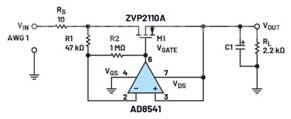
Figure 1. Active half-wave rectifier using a self-powered op amp

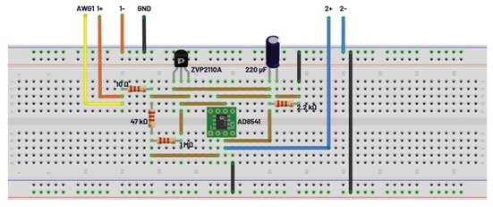
Figure 2. Active Half-Wave Rectifier Using a Self-Powered Op Amp Breadboard Circuit

When VINgreater than Voutthe op amp will turn on the PMOS transistor, with the following formula:
![]()

where (voltage referenced to ground):
VGATEis the voltage at the gate of M1.
VINFor AC input voltage.
Voutfor C1 and RLoutput voltage at .
The input and output voltages can be related to the PMOS drain-source voltage VDSand gate-source voltage VGSLinked together, the formula is as follows:
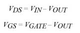

Combining these equations gives the MOSFET gate drive as a function of drain-source voltage:
![]()
If the value of R2 is 21 times that of R1 (1 MΩ/47 kΩ), the drain-source voltage of M1 VDSA 75 mV drop across is sufficient to turn on a PMOS transistor with a threshold voltage of C1.5 V. The ratio of R2 to R1 can be larger to reduce the input-to-output voltage drop or to support transistors with higher threshold voltages.
The op amp is powered by output smoothing capacitor C1, so no additional power supply is required. There are certain requirements for the op amp chosen for this circuit. The amplifier must have rail-to-rail inputs and outputs without gain-phase inversion when operating near the supply rails. The bandwidth of the op amp limits the frequency response of the circuit. Low supply current op amps are often chosen for this application to improve efficiency, so bandwidth and slew rates are typically lower. At higher AC input frequencies (probably higher than 500 Hz), the gain of the amplifier will start to drop. The AD8541 single-supply CMOS op amp meets all of these requirements with a supply current as low as 45 µA.
hardware settings
The breadboard connections for an active half-wave rectifier using a self-powered op amp are shown in Figure 2.
program steps
AWG1 is connected to VIN, should be configured as a sine wave with an amplitude greater than 6 V peak-to-peak, zero offset, and a frequency of 100 Hz. The oscilloscope input is used to monitor various points around the circuit, such as VINVoutRSvoltage across, and through RSand M1 gate current.
Start with a larger capacitor of 220 µF for C1. Both the 220 µF and 4.7 µF Capacitors are polarized, so be sure to connect the positive and negative ends correctly to the circuit.
Use the two oscilloscope inputs to monitor VINat the input AC waveform and VoutThe DC output waveform at . Voutshould be very close to VINPeak. Now replace the bulk 220 µF capacitor with a much smaller 4.7 µF capacitor. observe VoutThe waveform changes at. When Voutvalue closest to VINthe interval of the AC input cycle is compared with the gate voltage of transistor M1.
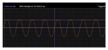
Figure 3. Using a 220 µF Capacitor for Voutand VIN Scopy diagram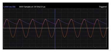
Figure 4. V Using a 4.7 µF Capacitoroutand VIN Scopy diagram


Oscilloscope channel 2 is connected at the shunt (i.e. 10 Ω resistor RS), use the measure feature to obtain the peak and average values of the current. Connect the average value with a 2.2 kΩ load resistor RLcompared with the DC value of VoutCalculated from the measured voltage. Repeat this measurement for the 220 µF and 4.7 µF capacitor values.
Other uses of this circuit
A circuit that only allows current to flow in one direction with a very low voltage drop across the switch has other potential uses. In a battery charger, where the input power may be intermittent (such as a solar panel or wind turbine generator), it is necessary to prevent the battery from discharging when the input power does not produce a high enough voltage to charge the battery. Simple Schottky diodes are typically used for this purpose, but as noted in the background section, this results in a loss of efficiency. Using an op amp with a sufficiently low operating supply current can often be lower than the reverse leakage current of a large Schottky diode.
question:
Can you name some practical applications of active rectifiers? You can find answers on the Student Zone forum.
About Analog Devices
Analog Devices, Inc. (NASDAQ: ADI) is the world’s leading semiconductor company dedicated to bridging the physical and digital worlds to enable breakthrough innovations at the intelligent edge. ADI provides solutions combining analog, digital and software technologies to promote the continuous development of digital factories, automobiles and digital medical care, address the challenges of climate change, and establish a reliable interconnection between people and everything in the world. ADI’s fiscal year 2022 revenue exceeds US$12 billion, with more than 24,000 employees worldwide. Together with 125,000 customers around the world, ADI helps innovators continue to exceed what is possible. For more information, visit www.analog.com/cn.
about the author
Doug Mercer graduated from Rensselaer Polytechnic Institute (RPI) in 1977 with a BSEE. Since joining Analog Devices in 1977, he has directly or indirectly contributed to more than 30 data converter products and holds 13 patents. He was named an ADI Fellow in 1995. In 2009, he transitioned from full-time employment and continues to serve as a consultant to ADI as an emeritus researcher, writing for the Active Learning Initiative. In 2016, he was appointed as the Engineer-in-Residence of the RPI ECSE Department. Contact: doug.mercer@analog.com.
Antoniu Miclaus is currently a System Applications Engineer at Analog Devices, working on ADI teaching projects and developing embedded software for Circuits from the Lab®, QA automation, and process management. He joined Analog Devices in February 2017 in Cluj-Napoca, Romania. He is currently an MSc student in the Software Engineering MSc program at Babes Bowyer University and holds a BSc in Electronics and Telecommunications Engineering from the Technical University of Cluj-Napoca. Contact: antoniu.miclaus@analog.com.
View more : IGBT modules | LCD displays | Electronic Components