“Many data acquisition, industrial control, and instrumentation applications require ultra-high-speed analog-to-digital converters (ADCs), and successive approximation register (SAR) converters fully meet this requirement. However, we must ensure that the external circuitry around the SAR converter is also up to the task to ensure successful conversion results.
“
Many data acquisition, industrial control, and instrumentation applications require ultra-high-speed analog-to-digital converters (ADCs), and successive approximation register (SAR) converters fully meet this requirement. However, we must ensure that the external circuitry around the SAR converter is also up to the task to ensure successful conversion results. For SAR converters, the key terminals that require special attention are their analog signal inputs – if not taken seriously, these input pins can create stability problems and capacitive charge “kickback”, resulting in inaccurate conversions and prolonged Signal acquisition time.
In SAR converter applications, the solution for precise control of the input signal lies in the driving of an operational amplifier (op amp). When paired with appropriate output Resistor and capacitor values, these devices are the basis for high-precision, robust solutions for high-resolution, 16-bit and 20-bit SAR converter systems.
This article will briefly discuss issues related to achieving stable and accurate SAR ADC conversions. Then, a suitable op amp to drive a SAR ADC is described, and how to implement the necessary input drive circuitry. We’ll use Analog Devices’ solution as an example.
SAR ADC input circuit
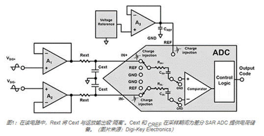
The SAR ADC driver circuit has operational amplifiers (A1 and A2) that isolate the ADC from its signal source (Figure 1). In this circuit, Rext is kept stable by isolating the output stage of the “isolated” amplifier from the ADC capacitive loads (CIN+ and CIN-) and Cext. Cext and CREF provide a near-perfect input source for the ADC to absorb switching charge injection from the IN+, IN-, and REF input terminals. The input terminals (IN+, IN-) track the voltage of the input signal (VSIG+, VSIG-) during the acquisition of the converter, charging the ADC input sampling Capacitors CIN+ and CIN-.


Taking Analog Device’s AD7915 (16-bit) and AD4021 (20-bit) SAR ADCs as examples to observe the inside of the ADC, it can be seen that the device uses a charge redistribution digital-to-analog converter (DAC). A capacitive DAC has two identical binary weighted capacitor arrays. These two capacitor arrays connect the non-inverting and inverting comparator inputs (Figure 2).
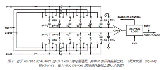

During the acquisition phase, the inputs (IN+ and IN-) are switched to the capacitor array. Additionally, SW+ and SW- are closed, connecting the least significant bit (LSB) capacitor to ground (GND). In this state, the capacitor array becomes the sampling capacitor, sampling the IN+ and IN- analog signals. After the acquisition phase is over, the CNV input of the control logic (right side) goes high to start the conversion phase.
The conversion phase begins by disconnecting SW+ and SW-, switching the two capacitor arrays to GND. In this configuration, the captured IN+ and IN- differential voltages cause the comparator to become unbalanced. The charge redistribution DAC methodically switches each element of the capacitor array from the most significant bit (MSB) to the LSB between GND and REF. The comparator inputs vary in binary weighted voltage steps (VREF/2N-1, VREF/2N-2…VREF/4, VREF/2). The control logic switches the switch from the MSB to the LSB, returning the comparator to a balanced state. After this process, the ADC returns to the acquisition phase and the control logic generates the ADC output codes.
Input Charge Injection, Circuit Stability, and Driving the AD7915 ADC
The key to the conversion process is to obtain an accurate input signal voltage. When the driver amplifier accurately charges the input capacitors CIN+ and CIN-, the ADC data conversion process proceeds smoothly and remains stable until the end of the ADC acquisition time. The problem for the designer is the introduction of a capacitor (CIN+, CIN-) at the input of the ADC and switching noise or “kickback” charge injection that needs to be managed by the driver amplifier.
Amplify the circuit Bode plot to quickly estimate circuit stability. The Bode plot tool can approximate the magnitude of the amplifier’s open-loop and system closed-loop gain transfer functions (Figure 3).
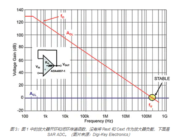

The y-axis quantifies the open-loop gain (AOL) and closed-loop gain (ACL) of the amplifier circuit, where the amplifier’s AOL curve starts at 130 decibels (dB) and the closed-loop gain ACL equals 0dB. Units along the X-axis quantify the open-loop and closed-loop gain frequencies from 100 hertz (Hz) to 1 gigahertz (GHz) in logarithmic form.
In Figure 3, the amplifier’s DC open-loop gain at about 220Hz (fO) drops from 130dB at a rate of -20dB/decade. This attenuation persists and crosses 0dB at approximately 180 megahertz (MHz) as the frequency increases. Since this curve represents a unipolar system, the divider frequency, fU, is equal to the gain-bandwidth product (GBWP) of the unity-gain stabilized amplifier. The graph represents a stable system because the cutoffs for AOL and ACL are 20dB/decade.
After adding Rext and Cext and the SAR ADC, modify the amplifier circuit by creating system zeros and poles (Figure 4). The system includes a 16-bit, 1 megatimes per second (MSPS) AD7915 differential PulSAR ADC and a 180 MHz, rail-to-rail input/output ADA4807-1 amplifier from Analog Devices. The combination of amplifier and ADC requires Rext due to the 30 picofarads (pF) (typ) ADC input capacitive loading. The circuit also requires Cext as a charging cartridge to provide enough charge at the ADC input to accurately match the input voltage.


As shown in Figure 4, oscillation is possible due to the capacitive loading of the ADC and the switching charge injection of the ADC during the initial acquisition of the circuit. The extra poles and zeros created by the Rext/Cext amplifier output components ensure system stability, so the intersection of the open-loop and closed-loop gain curves is greater than 20dB/decade, resulting in a phase margin of less than 45°. This configuration together with fP2 and fZ2 forms an unstable circuit.
To avoid instability, the designer needs to consider the effect of the amplifier’s open-loop output resistance, RO, when evaluating the open-loop gain curve of an amplifier with Rext and Cext in the circuit. The combination of RO and Rext, Cext with a resistance value of 50 ohms (W) modifies the open loop response curve by introducing a pole (fP, Equation 1) and a zero (fZ, Equation 2). The values of RO, Rext and Cext determine the corner frequency of fP. The values of Rext and Cext determine the zero corner frequency fZ.
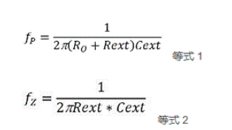

The calculation result of fP and fZ is:
fP1 = 842 kHz
fZ1 = 2.95 MHz
where: RO = 50 W
Rext = 20W
Cext = 2.7 nanofarads (nF)
fP2 = 22.7 MHz
fZ2 = 79.5 MHz
where: RO = 50 W
Rext = 20W
Cext = 0.1 nF
The above values of fP1 and fZ1 make the AD7915 and ADA4807-1 a stable system.
Driving Easy Drive AD4021 SAR ADC
An alternative to the AD7915 is the AD4021 20-bit 1 MSPS Easy Drive SAR converter. The AD4021 device family significantly reduces input kickback and input current to 0.5 microamps (μA)/MSPS. Easy Drive devices feature reduced power consumption and signal chain complexity.
The analog input of the AD4021 uses circuitry that reduces the nonlinear charge kickback of a typical switched capacitor SAR input. Lower bandwidth, lower power driver amplifiers can be used because of the reduced kickback and longer acquisition phase (Figure 5).


Reducing the kickback and extending the acquisition time also increases the Rext resistor value in the input resistor-capacitor (RC) filter and reduces the Cext capacitor accordingly. This combination of smaller Cext amplifier loads improves stability and reduces power consumption.
The recommended connection diagram for the AD4021 using a single 5V supply appears to have a similar circuit diagram. But the demands on the amplifier are reduced and the values of Rext/Cext (R and C) are smaller (Figure 6).


In Figure 6, the SAR-based AD4021 also uses a charge redistribution sampling DAC. The ADC has an onboard conversion clock and serial clock. Therefore, the synchronization clock (SCK) input is not required for the conversion process. This clock configuration extends acquisition time and improves accuracy by giving the input signal longer time to settle to its final value.
The main concern for the driver amplifiers of the AD7915 and AD4021 is noise, since the amplifier/Rext/Cext combination must step from full scale to the AD7915 at the 16-bit level (0.0015%, 15ppm), and the AD4021 at the 20-bit level (0.00001%, 1ppm) .
To maintain the signal-to-noise ratio (SNR) performance of the AD7915 and AD4021, the noise of the driver amplifier must be less than one-third the noise of the ADC. The noise of the AD4021 is 60 microvolts rms (mVrms), which requires the amplifier/Rext/Cext combination to have less than 20mVrms of noise. The noise of the AD4021 is 31.5 mVrms, which requires the amplifier/Rext/Cext combination to have less than 10.5 mVrms of noise.
Analog Devices’ precision ADC driver tools help designers quickly calculate the correct Rext and Cext values. With selected drivers and ADCs, the tool simulates the settling time, noise and distortion behavior of the circuit.
Epilogue
SAR ADCs will continue to dominate in ultra-high-speed data acquisition, industrial control, and instrumentation applications. However, we need to consider the external input circuitry of this type of device—the driver amplifier and input filter—to accommodate potential switching charge injection and amplifier stability issues.
Most solutions for SAR converters such as the AD7916 and AD4021 to precisely control the input signal rely on an op amp driver, such as the ADA4807-1 in this example. As shown, these types of devices, supported by appropriate output resistor and capacitor values, form a solid foundation upon which to build a high-accuracy, robust, high-resolution, 16- or 20-bit SAR converter system .
Many data acquisition, industrial control, and instrumentation applications require ultra-high-speed analog-to-digital converters (ADCs), and successive approximation register (SAR) converters fully meet this requirement. However, we must ensure that the external circuitry around the SAR converter is also up to the task to ensure successful conversion results. For SAR converters, the key terminals that require special attention are their analog signal inputs – if not taken seriously, these input pins can create stability problems and capacitive charge “kickback”, resulting in inaccurate conversions and prolonged Signal acquisition time.
In SAR converter applications, the solution for precise control of the input signal lies in the driving of an operational amplifier (op amp). When paired with appropriate output resistor and capacitor values, these devices are the basis for high-precision, robust solutions for high-resolution, 16-bit and 20-bit SAR converter systems.
This article will briefly discuss issues related to achieving stable and accurate SAR ADC conversions. Then, a suitable op amp to drive a SAR ADC is described, and how to implement the necessary input drive circuitry. We’ll use Analog Devices’ solution as an example.
SAR ADC input circuit
The SAR ADC driver circuit has operational amplifiers (A1 and A2) that isolate the ADC from its signal source (Figure 1). In this circuit, Rext is kept stable by isolating the output stage of the “isolated” amplifier from the ADC capacitive loads (CIN+ and CIN-) and Cext. Cext and CREF provide a near-perfect input source for the ADC to absorb switching charge injection from the IN+, IN-, and REF input terminals. The input terminals (IN+, IN-) track the voltage of the input signal (VSIG+, VSIG-) during the acquisition of the converter, charging the ADC input sampling capacitors CIN+ and CIN-.
Taking Analog Device’s AD7915 (16-bit) and AD4021 (20-bit) SAR ADCs as examples to observe the inside of the ADC, it can be seen that the device uses a charge redistribution digital-to-analog converter (DAC). A capacitive DAC has two identical binary weighted capacitor arrays. These two capacitor arrays connect the non-inverting and inverting comparator inputs (Figure 2).

During the acquisition phase, the inputs (IN+ and IN-) are switched to the capacitor array. Additionally, SW+ and SW- are closed, connecting the least significant bit (LSB) capacitor to ground (GND). In this state, the capacitor array becomes the sampling capacitor, sampling the IN+ and IN- analog signals. After the acquisition phase is over, the CNV input of the control logic (right side) goes high to start the conversion phase.
The conversion phase begins by disconnecting SW+ and SW-, switching the two capacitor arrays to GND. In this configuration, the captured IN+ and IN- differential voltages cause the comparator to become unbalanced. The charge redistribution DAC methodically switches each element of the capacitor array from the most significant bit (MSB) to the LSB between GND and REF. The comparator inputs vary in binary weighted voltage steps (VREF/2N-1, VREF/2N-2…VREF/4, VREF/2). The control logic switches the switch from the MSB to the LSB, returning the comparator to a balanced state. After this process, the ADC returns to the acquisition phase and the control logic generates the ADC output codes.
Input Charge Injection, Circuit Stability, and Driving the AD7915 ADC
The key to the conversion process is to obtain an accurate input signal voltage. When the driver amplifier accurately charges the input capacitors CIN+ and CIN-, the ADC data conversion process proceeds smoothly and remains stable until the end of the ADC acquisition time. The problem for the designer is the introduction of a capacitor (CIN+, CIN-) at the input of the ADC and switching noise or “kickback” charge injection that needs to be managed by the driver amplifier.
Amplify the circuit Bode plot to quickly estimate circuit stability. The Bode plot tool can approximate the magnitude of the amplifier’s open-loop and system closed-loop gain transfer functions (Figure 3).

The y-axis quantifies the open-loop gain (AOL) and closed-loop gain (ACL) of the amplifier circuit, where the amplifier’s AOL curve starts at 130 decibels (dB) and the closed-loop gain ACL equals 0dB. Units along the X-axis quantify the open-loop and closed-loop gain frequencies from 100 hertz (Hz) to 1 gigahertz (GHz) in logarithmic form.
In Figure 3, the amplifier’s DC open-loop gain at about 220Hz (fO) drops from 130dB at a rate of -20dB/decade. This attenuation persists and crosses 0dB at approximately 180 megahertz (MHz) as the frequency increases. Since this curve represents a unipolar system, the divider frequency, fU, is equal to the gain-bandwidth product (GBWP) of the unity-gain stabilized amplifier. The graph represents a stable system because the cutoffs for AOL and ACL are 20dB/decade.
After adding Rext and Cext and the SAR ADC, modify the amplifier circuit by creating system zeros and poles (Figure 4). The system includes a 16-bit, 1 megatimes per second (MSPS) AD7915 differential PulSAR ADC and a 180 MHz, rail-to-rail input/output ADA4807-1 amplifier from Analog Devices. The combination of amplifier and ADC requires Rext due to the 30 picofarads (pF) (typ) ADC input capacitive loading. The circuit also requires Cext as a charging cartridge to provide enough charge at the ADC input to accurately match the input voltage.

As shown in Figure 4, oscillation is possible due to the capacitive loading of the ADC and the switching charge injection of the ADC during the initial acquisition of the circuit. The extra poles and zeros created by the Rext/Cext amplifier output components ensure system stability, so the intersection of the open-loop and closed-loop gain curves is greater than 20dB/decade, resulting in a phase margin of less than 45°. This configuration together with fP2 and fZ2 forms an unstable circuit.
To avoid instability, the designer needs to consider the effect of the amplifier’s open-loop output resistance, RO, when evaluating the open-loop gain curve of an amplifier with Rext and Cext in the circuit. The combination of RO and Rext, Cext with a resistance value of 50 ohms (W) modifies the open loop response curve by introducing a pole (fP, Equation 1) and a zero (fZ, Equation 2). The values of RO, Rext and Cext determine the corner frequency of fP. The values of Rext and Cext determine the zero corner frequency fZ.

The calculation result of fP and fZ is:
fP1 = 842 kHz
fZ1 = 2.95 MHz
where: RO = 50 W
Rext = 20W
Cext = 2.7 nanofarads (nF)
fP2 = 22.7 MHz
fZ2 = 79.5 MHz
where: RO = 50 W
Rext = 20W
Cext = 0.1 nF
The above values of fP1 and fZ1 make the AD7915 and ADA4807-1 a stable system.
Driving Easy Drive AD4021 SAR ADC
An alternative to the AD7915 is the AD4021 20-bit 1 MSPS Easy Drive SAR converter. The AD4021 device family significantly reduces input kickback and input current to 0.5 microamps (μA)/MSPS. Easy Drive devices feature reduced power consumption and signal chain complexity.
The analog input of the AD4021 uses circuitry that reduces the nonlinear charge kickback of a typical switched capacitor SAR input. Lower bandwidth, lower power driver amplifiers can be used because of the reduced kickback and longer acquisition phase (Figure 5).

Reducing the kickback and extending the acquisition time also increases the Rext resistor value in the input resistor-capacitor (RC) filter and reduces the Cext capacitor accordingly. This combination of smaller Cext amplifier loads improves stability and reduces power consumption.
The recommended connection diagram for the AD4021 using a single 5V supply appears to have a similar circuit diagram. But the demands on the amplifier are reduced and the values of Rext/Cext (R and C) are smaller (Figure 6).

In Figure 6, the SAR-based AD4021 also uses a charge redistribution sampling DAC. The ADC has an onboard conversion clock and serial clock. Therefore, the synchronization clock (SCK) input is not required for the conversion process. This clock configuration extends acquisition time and improves accuracy by giving the input signal longer time to settle to its final value.
The main concern for the driver amplifiers of the AD7915 and AD4021 is noise, since the amplifier/Rext/Cext combination must step from full scale to the AD7915 at the 16-bit level (0.0015%, 15ppm), and the AD4021 at the 20-bit level (0.00001%, 1ppm) .
To maintain the signal-to-noise ratio (SNR) performance of the AD7915 and AD4021, the noise of the driver amplifier must be less than one-third the noise of the ADC. The noise of the AD4021 is 60 microvolts rms (mVrms), which requires the amplifier/Rext/Cext combination to have less than 20mVrms of noise. The noise of the AD4021 is 31.5 mVrms, which requires the amplifier/Rext/Cext combination to have less than 10.5 mVrms of noise.
Analog Devices’ precision ADC driver tools help designers quickly calculate the correct Rext and Cext values. With selected drivers and ADCs, the tool simulates the settling time, noise and distortion behavior of the circuit.
Epilogue
SAR ADCs will continue to dominate in ultra-high-speed data acquisition, industrial control, and instrumentation applications. However, we need to consider the external input circuitry of this type of device—the driver amplifier and input filter—to accommodate potential switching charge injection and amplifier stability issues.
Most solutions for SAR converters such as the AD7916 and AD4021 to precisely control the input signal rely on an op amp driver, such as the ADA4807-1 in this example. As shown, these types of devices, supported by appropriate output resistor and capacitor values, form a solid foundation upon which to build a high-accuracy, robust, high-resolution, 16- or 20-bit SAR converter system .
View more : IGBT modules | LCD displays | Electronic Components