更新时间:2021-11-28 03:20


The EMC mechanism that electronic engineers have to know-crosstalk
The EMC mechanism that electronic engineers have to know-crosstalk
[Guide]Crosstalk is one of the most basic phenomena in signal integrity. The influence of crosstalk is especially serious when the wiring density on the board is high. We know that the linear involuntary system satisfies the superposition theorem. If there is a signal transmission on the victim line, the noise caused by crosstalk will be superimposed on the signal on the victim line, thereby causing the signal to be distorted.

Figure 1. Crosstalk causes signal distortion
When crosstalk noise is superimposed on the high and low levels of the victim signal, amplitude noise will be generated or the eye height will be affected. When crosstalk noise is superimposed on the transition edge position of the victim signal, edge jitter will occur, which will affect the timing or the width of the eye diagram. From a statistical point of view, due to the uncertainty of the interference source, crosstalk noise generally affects the edge and amplitude of the signal at the same time. Therefore, for crosstalk, both effects should be considered.
The root cause of crosstalk is coupling. In a multi-conductor system, the conductors are coupled through electric and magnetic fields. This coupling transfers part of the signal’s energy to adjacent conductors, thereby creating noise. There are two main ways of coupling: 1. Capacitive coupling. 2. Inductive coupling.
Capacitive coupling
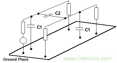
Recall the parallel plate capacitor we are familiar with. Two regular parallel plate conductors are filled with dielectric to form a capacitor. For the PCB board, a capacitor will also be formed between the two traces and between the reference plane. In Figure 3, C1 represents the capacitance formed between the trace and the reference plane, and C2 represents the capacitance formed between the two traces. From the perspective of capacitance, when the voltage on a trace changes, it is equivalent to the voltage across the capacitor C2. The adjacent conductor (the other end of the capacitor) charged by the capacitor C2 will inevitably have current, and crosstalk will occur. The capacitance between the traces is closely related to the spacing between the traces. When the spacing increases, the coupling capacitance decreases rapidly, and the coupling effect decreases sharply. If another trace is placed between the two traces, the coupling capacitance between the two jump traces will be further reduced. This phenomenon is one of the starting points for using the isolation bottom line to suppress crosstalk.


Figure 2. Capacitive coupling
Inductive coupling
If there is a digital signal transmission on a trace, during the signal level transition, that is, when the signal is on the edge of the transition, the voltage on the trace continuously changes, and the current on the trace also continuously changes, thus causing changes around the trace The magnetic field, and the changing magnetic field induces current in adjacent traces. This is inductive coupling. The same distance between the traces on the PCB board can significantly reduce the mutual inductance coupling between the two antennas. The inductive coupling mechanism is shown in Figure 3


Figure 3. Inductive coupling
The Links:
dmf-50840nf-fw-aue-bin
pm20cha060
The EMC mechanism that electronic engineers have to know-crosstalk
[Guide]Crosstalk is one of the most basic phenomena in signal integrity. The influence of crosstalk is especially serious when the wiring density on the board is high. We know that the linear involuntary system satisfies the superposition theorem. If there is a signal transmission on the victim line, the noise caused by crosstalk will be superimposed on the signal on the victim line, thereby causing the signal to be distorted.
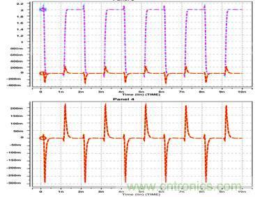
Figure 1. Crosstalk causes signal distortion
When crosstalk noise is superimposed on the high and low levels of the victim signal, amplitude noise will be generated or the eye height will be affected. When crosstalk noise is superimposed on the transition edge position of the victim signal, edge jitter will occur, which will affect the timing or the width of the eye diagram. From a statistical point of view, due to the uncertainty of the interference source, crosstalk noise generally affects the edge and amplitude of the signal at the same time. Therefore, for crosstalk, both effects should be considered.
The root cause of crosstalk is coupling. In a multi-conductor system, the conductors are coupled through electric and magnetic fields. This coupling transfers part of the signal’s energy to adjacent conductors, thereby creating noise. There are two main ways of coupling: 1. Capacitive coupling. 2. Inductive coupling.
Capacitive coupling
Recall the parallel plate capacitor we are familiar with. Two regular parallel plate conductors are filled with dielectric to form a capacitor. For the PCB board, a capacitor will also be formed between the two traces and between the reference plane. In Figure 3, C1 represents the capacitance formed between the trace and the reference plane, and C2 represents the capacitance formed between the two traces. From the perspective of capacitance, when the voltage on a trace changes, it is equivalent to the voltage across the capacitor C2. The adjacent conductor (the other end of the capacitor) charged by the capacitor C2 will inevitably have current, and crosstalk will occur. The capacitance between the traces is closely related to the spacing between the traces. When the spacing increases, the coupling capacitance decreases rapidly, and the coupling effect decreases sharply. If another trace is placed between the two traces, the coupling capacitance between the two jump traces will be further reduced. This phenomenon is one of the starting points for using the isolation bottom line to suppress crosstalk.


Figure 2. Capacitive coupling
Inductive coupling
If there is a digital signal transmission on a trace, during the signal level transition, that is, when the signal is on the edge of the transition, the voltage on the trace continuously changes, and the current on the trace also continuously changes, thus causing changes around the trace The magnetic field, and the changing magnetic field induces current in adjacent traces. This is inductive coupling. The same distance between the traces on the PCB board can significantly reduce the mutual inductance coupling between the two antennas. The inductive coupling mechanism is shown in Figure 3
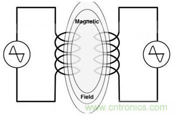

Figure 3. Inductive coupling
The Links:
dmf-50840nf-fw-aue-bin
pm20cha060
The EMC mechanism that electronic engineers have to know-crosstalk
[Guide]Crosstalk is one of the most basic phenomena in signal integrity. The influence of crosstalk is especially serious when the wiring density on the board is high. We know that the linear involuntary system satisfies the superposition theorem. If there is a signal transmission on the victim line, the noise caused by crosstalk will be superimposed on the signal on the victim line, thereby causing the signal to be distorted.

Figure 1. Crosstalk causes signal distortion
When crosstalk noise is superimposed on the high and low levels of the victim signal, amplitude noise will be generated or the eye height will be affected. When crosstalk noise is superimposed on the transition edge position of the victim signal, edge jitter will occur, which will affect the timing or the width of the eye diagram. From a statistical point of view, due to the uncertainty of the interference source, crosstalk noise generally affects the edge and amplitude of the signal at the same time. Therefore, for crosstalk, both effects should be considered.
The root cause of crosstalk is coupling. In a multi-conductor system, the conductors are coupled through electric and magnetic fields. This coupling transfers part of the signal’s energy to adjacent conductors, thereby creating noise. There are two main ways of coupling: 1. Capacitive coupling. 2. Inductive coupling.
Capacitive coupling
Recall the parallel plate capacitor we are familiar with. Two regular parallel plate conductors are filled with dielectric to form a capacitor. For the PCB board, a capacitor will also be formed between the two traces and between the reference plane. In Figure 3, C1 represents the capacitance formed between the trace and the reference plane, and C2 represents the capacitance formed between the two traces. From the perspective of capacitance, when the voltage on a trace changes, it is equivalent to the voltage across the capacitor C2. The adjacent conductor (the other end of the capacitor) charged by the capacitor C2 will inevitably have current, and crosstalk will occur. The capacitance between the traces is closely related to the spacing between the traces. When the spacing increases, the coupling capacitance decreases rapidly, and the coupling effect decreases sharply. If another trace is placed between the two traces, the coupling capacitance between the two jump traces will be further reduced. This phenomenon is one of the starting points for using the isolation bottom line to suppress crosstalk.

Figure 2. Capacitive coupling
Inductive coupling
If there is a digital signal transmission on a trace, during the signal level transition, that is, when the signal is on the edge of the transition, the voltage on the trace continuously changes, and the current on the trace also continuously changes, thus causing changes around the trace The magnetic field, and the changing magnetic field induces current in adjacent traces. This is inductive coupling. The same distance between the traces on the PCB board can significantly reduce the mutual inductance coupling between the two antennas. The inductive coupling mechanism is shown in Figure 3

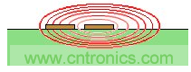
Figure 3. Inductive coupling
[Guide]Crosstalk is one of the most basic phenomena in signal integrity. The influence of crosstalk is especially serious when the wiring density on the board is high. We know that the linear involuntary system satisfies the superposition theorem. If there is a signal transmission on the victim line, the noise caused by crosstalk will be superimposed on the signal on the victim line, thereby causing the signal to be distorted.

Figure 1. Crosstalk causes signal distortion
When crosstalk noise is superimposed on the high and low levels of the victim signal, amplitude noise will be generated or the eye height will be affected. When crosstalk noise is superimposed on the transition edge position of the victim signal, edge jitter will occur, which will affect the timing or the width of the eye diagram. From a statistical point of view, due to the uncertainty of the interference source, crosstalk noise generally affects the edge and amplitude of the signal at the same time. Therefore, for crosstalk, both effects should be considered.
The root cause of crosstalk is coupling. In a multi-conductor system, the conductors are coupled through electric and magnetic fields. This coupling transfers part of the signal’s energy to adjacent conductors, thereby creating noise. There are two main ways of coupling: 1. Capacitive coupling. 2. Inductive coupling.
Capacitive coupling
Recall the parallel plate capacitor we are familiar with. Two regular parallel plate conductors are filled with dielectric to form a capacitor. For the PCB board, a capacitor will also be formed between the two traces and between the reference plane. In Figure 3, C1 represents the capacitance formed between the trace and the reference plane, and C2 represents the capacitance formed between the two traces. From the perspective of capacitance, when the voltage on a trace changes, it is equivalent to the voltage across the capacitor C2. The adjacent conductor (the other end of the capacitor) charged by the capacitor C2 will inevitably have current, and crosstalk will occur. The capacitance between the traces is closely related to the spacing between the traces. When the spacing increases, the coupling capacitance decreases rapidly, and the coupling effect decreases sharply. If another trace is placed between the two traces, the coupling capacitance between the two jump traces will be further reduced. This phenomenon is one of the starting points for using the isolation bottom line to suppress crosstalk.


Figure 2. Capacitive coupling
Inductive coupling
If there is a digital signal transmission on a trace, during the signal level transition, that is, when the signal is on the edge of the transition, the voltage on the trace continuously changes, and the current on the trace also continuously changes, thus causing changes around the trace The magnetic field, and the changing magnetic field induces current in adjacent traces. This is inductive coupling. The same distance between the traces on the PCB board can significantly reduce the mutual inductance coupling between the two antennas. The inductive coupling mechanism is shown in Figure 3


Figure 3. Inductive coupling