Texas Instruments (TI) has expanded its family of high-speed data converters with a new family of eight successive-approximation register (SAR) analog-to-digital converters (ADCs) that enable high-speed data acquisition in industrial environments. Targeting real-time control challenges in industrial systems, the ADC3660 SAR ADCs in 14-, 16- and 18-bit resolution at sampling speeds ranging from 10 to 125 MSPS claim to reduce power consumption by 65 percent and lower latency by 80 percent compared with competitive devices.
During a press conference, Matt Hann, product line manager, high-speed data converters at TI, highlighted the need for real-time control in industrial systems, and thus the importance of the new ADC3660 family not only in the realm of real-time control, but also in terms of precision and high speed.
Until now, engineers designing industrial systems have had to choose between various compromises in terms of noise and low power consumption – a particularly difficult decision for those designing battery-powered devices that require precise data acquisition. Hann pointed out that the ADC3660 family aims to address these trade-offs and other challenges including accuracy, size, and design time.
“What we’re bringing to the table now that wasn’t present before is a marriage of accuracy, noise, power, size, and features that make it very easy for these devices to get designed into a system,” said Hann. “There are devices that have existed at this sampling rate in the market, but what we brought to the table is better noise performance at that sampling rate and resolution, as well as integrated digital features and lowest power consumption.”
Digital control in real-time
Increasing accuracy in high-speed data acquisition meets a growing industrial need for real-time control. Here, in a high-speed digital control loop, the ADC acts in a complex system to respond to rapid voltage or current changes and helps prevent costly damage to critical components in power management systems.
“When you talk about real time, you think of something instantaneous,” said Hann. So, in a real-time control system, instantaneous control is often needed where high precision and speed are important, such as in thermal imaging cameras, network infrastructures, power quality analyzers, plasma cutters, and source measurement units, he added.

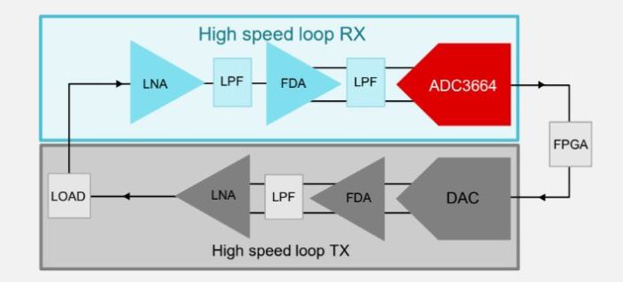
Fig. 1: Enabling real-time control with digital control loops (Source: TI)
As shown in Fig. 1, there are four key pieces to the digital control loop. In the high-speed loop RX, there is an analog signal chain that brings the data to the ADC, in this case the ADC3664, which is processed by an FPGA, a real-time microcontroller (MCU) or even a DSP, and that information is taken and translated back to the load by a DAC, said Hann. “The total amount of time it takes for this to happen is measured by what we call latency. So, in the past low latency was something that only an analog control loop could enable because you weren’t limited necessarily by the sampling rate of the ADC, or even the noise of the ADC making an accurate measurement,” said Hann.
TI’s new ADC offers nanosecond latency, providing not only real-time control but also design flexibility. “What enables a digital controller to be flexible is the programmability that the ADC3664 offers,” said Hann.
Real-time tuneability and programmability allow an end designer to customize a system that can adapt to multiple applications by simply changing a few parameters in the software, said Hann. “That results in flexibility for the end design and a lot of cost savings for the end customer.”
SAR ADCs
Hann highlighted a few devices in the new family of ADCs, which consist of eight pin-to-pin compatible devices in single- or dual-channel configurations, ranging from 10 to 125 MSPS in 14-, 16- and 18-bit resolutin grades. Depending on the device, the family can offer up to 80 percent lower latency for real-time control and best-in-class dynamic range at the lowest power consumption, as well as integrated features and high sampling frequencies that make design very easy, he said.
One example is the ADC3683, which TI claimed as the industry’s fastest 18-bit ADC. “The ADC3683 is a 65-MSPS, 18-bit dual-channel ADC and it samples four times faster than the closest competing 18-bit device at twice the channel density,” said Hann. “It improves noise performance in narrowband frequency applications such as portable defense radios with a signal-to-noise ratio (SNR) of 84.2 dB and noise spectral density of -160 dBFS/Hz. Moreover, it consumes less power at 94 mW per channel and enables high precision data acquisition systems such as source measurement units and other types of handheld instrumentation,” said Hann.

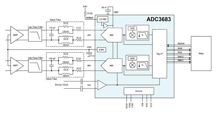
Fig. 2: Application diagram of ADC3683 (Source: TI)
The 125-MSPS, 14-bit, dual-channel ADC3664 (noted earlier) is another variant, which delivers low latency (1 clock, 8 ns) and helps safeguard critical components and increase tool precision in applications like Semiconductor manufacturing systems. The devices’s ultra-low latency enables high-speed digital control loops in a wide variety of industrial systems to more accurately monitor and respond to voltage and current spikes.
This specific variant delivers 80 percent lower latency, which is lower than competitive devices at similar speeds including SAR and pipeline architecture ADCs, said Hann.

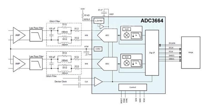
Fig. 3: Application diagram of ADC3664 (Source: TI)
In terms of low power consumption, the 65-MSPS, 16-bit ADC3660 delivers ultra-low-noise at 82 dBFS SNR, improving image resolution in sonar applications while consuming 65 percent less power (71 mW per channel) than the equivalent competitive device, said Hann.
“For an application like sonar with 65 percent less power it is a very compelling device and also the 65-MSPS, 16-bit dual channel makes it ideal and can oftentimes eliminate extra signal chain components in the in the path because of that low power consumption,” he said. “Eliminating the signal chain path can also reduce the overall system power consumption.”

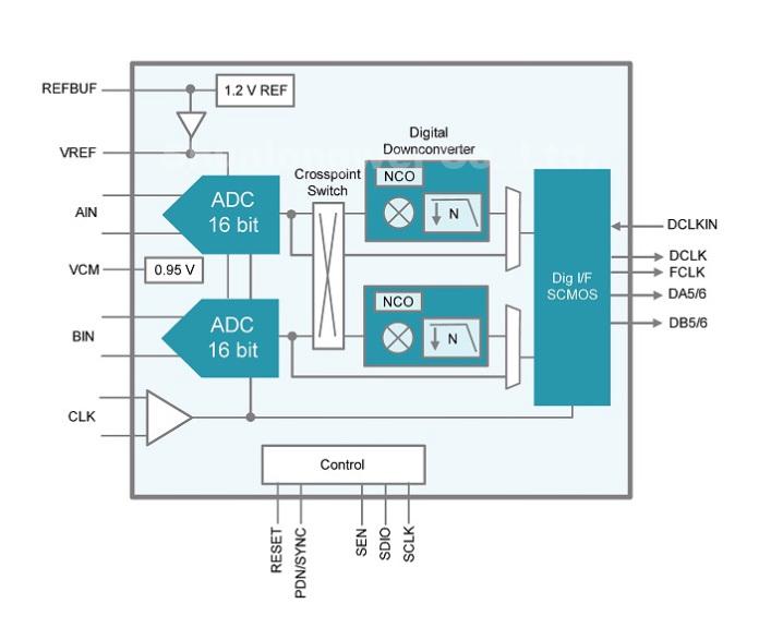
Fig. 4: Functional block diagram of the ADC3660 (Source: TI)
Reducing design complexity
The ADC3660 family’s high sampling rates and integrated features help designers reduce the number of components in their systems. For example, the ADC3683 allows oversampling, which pushes harmonics further away from the desired signal. This allows designers to reduce the complexity of the antialiasing filter and the number of components in the system by up to 75 percent.
Other family features that reduce design complexity include on-chip decimation options that allow designers to remove unwanted noise and harmonics in the system and increase the SNR and spurious-free dynamic range by up to 15 dB. These decimation options and the CMOS interface allow designers to use these ADCs with Arm-based processors or DSPs instead of FPGAs, which can help reduce system cost.
“We’re bringing the compute functionality from the processor into the ADC and this scales down system costs with either an Arm-based processor or a DSP and it increases the system functionality by being able to leverage processor resources for other tasks,” said Hann.
The ADC3563, ADC3583, ADC3643, ADC3660, ADC3663, ADC3664 and ADC3683 devices are available now from TI in a 5 ×5-mm very thin quad flat no-lead (WQFN) package. Pre-production versions of the ADC3541 are available now, only on TI.com, with volume production expected in the first quarter of 2022. Available now from TI, evaluation modules are priced at $249.
about Texas Instruments