Toshiba’s New Technology for SiC Power Modules Improves Reliability and Reduces Size
TOKYO–Toshiba Electronic Devices & Storage Corporation (“Toshiba”) has developed package technology for silicon carbide (SiC) power modules that doubles their reliability [1] and reduces their footprint by 20%[2].
SiC realizes higher voltages and lower losses than silicon, and is widely seen as the next-generation material for power devices. While use now centers on inverters for trains, wider deployment in high-voltage applications is on the horizon, including in photovoltaic power systems and automotive equipment.
Reliability is the main concern that has limited use of SiC devices. Application in high voltage power modules requires that not only the Semiconductor chip but also the package itself delivers high-level reliability. Toshiba has achieved this with a new silver (Ag) sintering technology for die bonding.
With current SiC packages, it is difficult to suppress increased on-resistance in chips over time, as higher power densities and switching frequencies trigger deterioration in their soldering. Ag sintering significantly reduces this deterioration. The thermal resistance in the Ag-sintered layer is also half that of a soldered layer, which allows chips in the module to be positioned closer together, realizing a smaller footprint.
Toshiba has dubbed the new package iXPLV, and will apply it to mass production of 3.3kV class SiC power module from the end of this month. Details of the technology were reported on May 5 at PCIM Europe, an international power semiconductor conference held online.
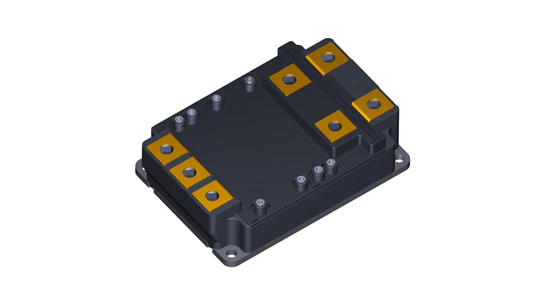
The new package for the SiC power module (iXPLV)

Note
[1] Toshiba defines reliability as the length of time until the occurrence of a 5% voltage change in a power cycling test, a recognized test of semiconductor reliability. For an Ag-sintered module, the time is approximately two times longer than for Toshiba’s soldered module.
[2] The new package has a 140×100mm footprint, 23% smaller than that of Toshiba’s current 140×130mm package.
[3] The X axis in the graph is the relative number of times that a set cycles between being on or off. The power cycle test evaluates deterioration of the semiconductor after numerous cycles. Toshiba defines the number of cycles that results in a 5% voltage change in the solder module as “1”.
- Customer Inquiries:
-
Power Device Sales & Marketing Department
Tel: +81-3-3457-3416


*Company names, product names, and service names may be trademarks of their respective companies.
*Information in this document, including product prices and specifications, content of services and contact information, is current on the date of the announcement but is subject to change without prior notice.