Wide bandgap (WBG) power semiconductors are being adopted into mainstream designs due to order-of-magnitude improvements in electrical figures-of-merit (FOMs). These huge performance improvements require revisiting many design assumptions, including thermal management [1].
This article discusses the challenges that thermal management raises due to increased power density, especially with chip-scale-packaging (CSP). What is sometimes overlooked, however, is that CSP eGaN® power FETs and integrated circuits have excellent thermal performance when mounted on standard printed circuit boards (PCBs) with simple methods for attaching heat sinks.
For example, a CSP GaN FET with a 4 mm2 footprint on a standard 4-layer pcb can achieve junction-to-heat sink thermal resistance values of less than 4 K/W with low-cost assembly and heat sink materials and techniques. Analysis, simulation, and experimental verification are provided in this article. In addition, pathways to further thermal improvement are discussed.
As an example, consider the case of a surface mount buck converter synchronous rectifier, where the dominant loss is conduction loss. A CSP eGaN FET, the EPC2059, occupies 3.92 mm2 of PCB area for a 170V, 9 mΩ FET, whereas a state-of-the-art 150V, 16.5 mΩ doubleside cooled Si MOSFET occupies nearly eight times the board PCB area at 30.9 mm2.
If footprint area were the dominant factor determining temperature rise, the larger Si mosfet would have a temperature rise about 23% of that of a GaN for a given current, even though the eGaN FET has much lower on-resistance (RDS(on)). In practice, however, the thermal performance of CSP eGaN FETs appear to be on par with, or better than, larger Si MOSFETs. This seemingly counter-intuitive result, and the reasons for it, are not obvious, hence some in-depth investigation is required.
Several publications demonstrate that chip-scale eGaN FETs have excellent absolute thermal performance despite their much smaller area compared to equivalent RDS(on) mosfets, and that practical heat sink mounting methods exist [2, 3] as illustrated in Figure 1 that shows a simple method for attaching a heat sink to CSP eGaN FETs. Unfortunately, most publications provide little detail on heat flow and the thermal models, when present. The articles are simplistic and have little rigorous justification.
Since the maximum rated junction temperature, Tj,max, is often the main limiting factor in designs, it is crucial for power systems designers to understand how and why high thermal performance can be achieved. Such understanding provides confidence in design; thus, shortening design cycles, reducing the amount and severity of required testing, increasing reliability, and reducing overall cost.
In many designs using surface mount power semiconductors, the PCB and the Transistor-to-heat sink interface form the first bottleneck to heat flow [4]. In cases where a heat sink is used, the PCB’s role in heat dissipation is frequently neglected, but is, in fact, a significant path for heat flow. The PCB’s contribution to extracting heat is significant even for very small CSP eGaN FETs where, in practical designs, such FETs can achieve thermal performance from junction-to-ambient on par with, or even better than, much larger Si MOSFETs.
When combined with the superior electrical performance of eGaN FETs, size can be reduced, power levels increased, and operating temperatures lowered. This can be shown using detailed 3D finite element simulations of typical PCB layouts in conjunction with experimental verification.
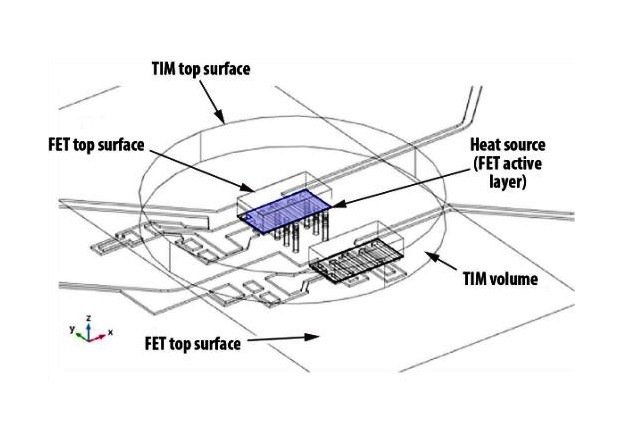
For high power applications, or those that operate in environments with a high ambient temperature, heat sinks are used to transfer the heat energy to the ambient environment. A typical thermal management approach for a CSP eGaN FET involves the application of an electrically insulating thermal interface material (TIM) to the top surface of the mounted FET, and mechanically attaching a heat sink atop it. In this configuration, spacers are often used to ensure that the heat sink has sufficient distance from the FET’s top surface to the facing surface of the heat sink in order to meet both voltage standoff requirements and absorb mechanical variations, as shown in Figure 1.
Figure 2 shows the various heat flow paths for the thermal assembly previously described. Intuitively, it appears that heat flow from the top and sides of the chip-scale FET dominates due to the short path through the TIM, whereas, in fact, the heat flow following the PCBTIM-heat sink path is also a large contributor to heat removal.
Due to the solder metallic bond, the FET has an excellent thermal connection with the copper on the PCB. The PCB effectively spreads the heat since the thermal conductivity of the copper is approximately two orders of magnitude higher than the TIM. Though the heat from the PCB to the heat sink must flow through a TIM thickness 2-5 times larger than the path from the FET to the heat sink, the effective crosssection of TIM in this path may be greater than 10 times the exposed surface area of the FET, since its area is proportional to the square of the radius of the cylinder formed by the application of the thermal interface material. Hence, the contribution of the PCB-to-heat sink thermal path must be taken into account when analyzing this thermal management approach.

The above analysis can be accomplished using 3D finite element method (FEM) tools. A half-bridge PCB for eGaN FETs forms the baseline case. This PCB has a layout optimized for best electrical performance [5] and uses 4-layer construction of 70 mm copper foil, FR408 dielectric, and has a total thickness of 1.6 mm (62 mils). A volume of thermally conductive putty is placed on the mounted FETs and immediate vicinity as shown in Figure 3. A heat sink is placed over the FETs with a gap between the top side of the FET and facing heat sink surface. The board has copper pours with insulating gaps and a subset of vias that would be used in a typical design. A key point is that the best electrical performance drives the designer to put as much copper in the immediate vicinity of the FET, which also benefits the thermal performance.
| TIM part number | Thermal conductivity [W/m/K] |
Power [W] |
ΔT [K] (FET to spreader) |
Measured Rθ [K/W] |
Simulated Rθ [K/W] |
| 65-00-GEL30-0010 | 3.5 | 1.06 | 6.62 | 6.2 | 6.1 |
| TG-PP10-50G | 10 | 5.06 | 25.6 | 5.1 | 5.1 |
Table I: Thermal Interface Materials (TIM) Used in Experiments Reported in This Article
Experimental Results A series of physical experiments were conducted to verify these simulations and to further understand the practical effects on the FET, such as thermal contact impedance. Good agreement among the empirical results and the simulations was obtained, which supported confidence in the simulations.
A cost analysis was done with the more expensive 10 W/m/K (TGPP10-50G) material. A 10 mm diameter cylinder of material surrounding the FET has approximately 70 ml volume. For moderate production rates, the per-FET TIM cost is less than $0.01 US.
Summary
Small chip-scale eGaN FETs have excellent thermal performance when mounted on a PCB that is designed for best electrical performance. This performance is obtained with simple, manufacturable, and cost-effective thermal solutions.