A Technical Analysis of the Infineon F3L150R07W2E3_B11 Three-Level IGBT Module
“`html
Infineon F3L150R07W2E3_B11 Three-Level IGBT Module | 650V 150A
Technical Analysis of the F3L150R07W2E3_B11 IGBT Module
The Infineon F3L150R07W2E3_B11 is a three-level Neutral Point Clamped (NPC2) IGBT module engineered for high-efficiency power conversion. Its core value proposition lies in the integration of the advanced NPC2 topology with Infineon’s proven TRENCHSTOP™ IGBT3 technology, resulting in significantly lower switching losses and improved output voltage quality. This module is designed for systems that demand high power density and superior thermal performance.
- Core Specifications: 650V | 150A | VCE(sat) (typ) 1.50V
- Key Advantages: Reduced harmonic distortion, enhanced inverter efficiency.
- Assembly Benefit: Simplified, reliable mounting with PressFIT contact technology.
By splitting the DC-link voltage across multiple devices, the three-level topology halves the voltage stress on each IGBT, which directly lowers switching losses and enables operation at higher frequencies. Download Official Datasheet (PDF)


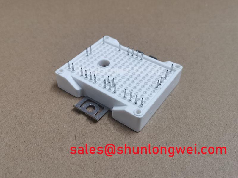
Advanced Topology for Superior Performance
The defining feature of the F3L150R07W2E3_B11 is its three-level NPC2 topology. In conventional two-level inverters, switches must block the full DC bus voltage. The NPC2 design halves this requirement for each device. This reduction in blocking voltage allows for the use of lower-voltage, faster-switching IGBTs. The engineering result is a substantial decrease in switching losses and a cleaner, near-sinusoidal output waveform with less electromagnetic interference (EMI). This makes the module an excellent component for systems where efficiency and grid-compatibility are paramount. For a deeper understanding, explore our guide to multi-level inverter topologies.
Thermal Efficiency and Conduction Losses
This module integrates Infineon’s TRENCHSTOP™ IGBT3, a technology known for its low collector-emitter saturation voltage (VCE(sat)), which is specified at a typical value of 1.50V at 150A and 25°C. This parameter directly impacts conduction losses—the primary source of heat generation when the device is on. A lower VCE(sat) means less power is wasted as heat. This is coupled with a low thermal resistance from junction to case (RthJC) of 0.17 K/W per IGBT. You can think of thermal resistance as the width of a pipe for heat flow; a lower value signifies a wider pipe, allowing heat to escape more efficiently to the heatsink. This efficient thermal pathway is critical for ensuring the module operates below its maximum junction temperature of 175°C, even under heavy loads.
Optimized Application Scenarios
The specific characteristics of the F3L150R07W2E3_B11 make it highly suitable for select applications:
- Solar Inverters: The three-level topology generates a cleaner AC output with lower Total Harmonic Distortion (THD), improving grid compatibility and maximizing energy harvest.
- Uninterruptible Power Supplies (UPS): Its high efficiency, driven by low switching and conduction losses, reduces cooling requirements and overall system operating costs.
- Industrial Motor Drives: The smoother output waveform reduces motor torque ripple and audible noise, leading to better performance in precision motor control systems.
Its architecture is an optimal match for high-frequency power conversion systems requiring superior efficiency and low electromagnetic interference.
Key Specifications of the F3L150R07W2E3_B11
| Absolute Maximum Ratings (Tj = 25°C unless otherwise specified) | ||
|---|---|---|
| Parameter | Symbol | Value |
| Collector-emitter Voltage | VCES | 650 V |
| Continuous DC Collector Current (TC = 25°C, Tvj max = 175°C) | IC | 150 A |
| Repetitive Peak Collector Current (tp = 1 ms) | ICRM | 300 A |
| Gate-emitter Peak Voltage | VGES | +/-20 V |
| Electrical & Thermal Characteristics (IGBT) | ||
| Collector-emitter Saturation Voltage (IC=150A, VGE=15V, Tvj=25°C) | VCE(sat) | 1.50 V (typ) |
| Total Switching Energy (IC=150A, VCE=300V, VGE=±15V, Rg=5.1Ω, Tvj=125°C) | Ets | 15.5 mJ (typ) |
| Thermal Resistance, Junction to Case (per IGBT) | RthJC | 0.17 K/W |
| Operating Junction Temperature | Tvj op | -40 to +175°C |
Engineer’s FAQ for F3L150R07W2E3_B11
1. What are the primary advantages of the F3L150R07W2E3_B11’s three-level NPC2 topology compared to a standard two-level module?
The main benefits are improved efficiency and power quality. By reducing the switched voltage by 50%, switching losses are significantly decreased. This also results in lower dV/dt stress, which reduces EMI generation. The output voltage has more steps, creating a smoother sine wave with less harmonic distortion.
2. What mounting considerations are necessary for the PressFIT pins on this EconoPACK™ 3 module?
PressFIT technology provides a reliable, solder-free connection. A key consideration is the printed circuit board (PCB) hole specification. The datasheet provides precise details on the required finished hole diameter and plating thickness. Using a proper press-in tool is essential to apply even force and ensure a secure, gas-tight connection without damaging the pins or the PCB. Proper mechanical support for the PCB during insertion is also critical.
3. The datasheet specifies a maximum operating junction temperature (Tvj op) of 175°C. How should this influence thermal design?
The 175°C rating provides significant headroom for thermal management. It allows for higher power density or operation in demanding ambient conditions. However, designing a system to continuously operate near this limit is not recommended as it can reduce lifetime. An effective thermal design, using the module’s specified RthJC, should aim to keep the operating junction temperature well below this maximum to ensure long-term reliability. An integrated NTC provides the necessary feedback for precise thermal monitoring and protection.
Enabling Efficient Power Conversion
The F3L150R07W2E3_B11 module provides a robust, high-performance solution for power system designers. Its combination of a loss-reducing three-level topology, efficient TRENCHSTOP™ IGBT3 silicon, and a reliable, easy-to-mount package empowers engineers to develop more compact, efficient, and reliable power converters.
“`