
Made using Semiconductor lithography techniques, the capacitors are intended for high-end applications such as in-package power supply decoupling for mobiles and high-performance computing.
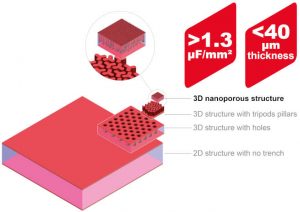
The main change in the process is a different 3D structure with larger electrode area, plus another change opening the door to different dielectrics.
“The extremely low ESL – a few pH – and low ESR – a few mΩ – of these devices support the highest performance power distribution networks that require low impedance over a wide frequency bandwidth,” according to the company.
With its thinness and high capacitance, specific in-package locations like land side mounting are possible, shortening the distance between the capacitance and active device.
It will be a while before standard products are available from the process.
“We’re speaking here about a new technology generation that will serve multiple product ranges,” a company spokesperson told Electronics Weekly. “For the time being, it is used for custom products designed especially for specific customer requirements. Some are single capacitors, some are integrated passive devices with several capacitances in the same package.”