At present, semiconductor laser (LD) has been widely used in many fields such as communication, information inspection, medical treatment and precision processing and military. The laser power supply is an important part of the laser device, and its performance directly affects the technical indicators of the entire laser device. This design uses a constant current source controlled by DSP to provide current for the semiconductor laser. In the circuit, the principle of negative feedback is used to control the output current of the composite power regulator to achieve the purpose of stabilizing the output current. The system uses a combination of circuit design and program control algorithm design to detect and control the working status of the semiconductor laser in real time from many aspects, so that the performance of the system is greatly improved and improved, and effectively solves the accuracy of the semiconductor laser. , Stability and reliability issues have further improved the output indicators of semiconductor lasers.
System principle
To make the laser output a laser with a stable wavelength, the current flowing through the laser is required to be very stable, so the power supply circuit selects a low-noise, stable constant current source. The constant current source current can be continuously adjusted between 0A and 3A to adapt to different specifications of lasers. At present, the secondary development of semiconductor laser power supplies generally adopts pure hardware circuit systems or single-chip control. With embedded micro-processing With the rapid development of DSP, digital control based on DSP can more effectively solve the problems of stability, accuracy and reliability of semiconductor laser work. The principle of the secondary development of DSP is shown in Figure 1.
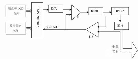
Figure 1 System schematic diagram

The voltage control signal output by the DSP is output to the operational amplifier, which is amplified by the operational amplifier and output to control the composite regulator composed of the triode 8050 and the regulator TIP122. The emitter of the regulator tube is connected in series with a Relay and a high-power sampling Resistor. Take the voltage signal from both ends of the sampling resistor and send it to the differential amplifier circuit U2 to obtain the voltage on the sampling resistor. This voltage signal passes through a voltage follower and enters the analog signal input channel of the ADC controlled by the DSP. The ADC converts the input analog signal into a digital signal, and then the DSP performs data processing on the converted digital signal. The sampling resistor is a high-power metal film resistor of 0.15Ω, which requires a good temperature coefficient. The amplification factor of the operational amplifier U1 determines the current control accuracy. The smaller the amplification factor, the higher the current output accuracy. At the same time, the amplification factor of the differential feedback circuit U2 will also affect the control accuracy of the current. The larger the amplification factor, the higher the stability of the current, but the output range of the current becomes smaller. In the case of a certain control voltage, the accurate selection of the multiple of the operational amplifier U1 and the multiple of the differential feedback circuit U2 will become an important factor in determining the current output accuracy and current output range of the constant current source.
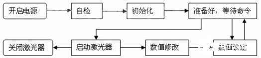
Figure 2 System workflow

TMS320F2812 control system
The design circuit is based on the digital signal processor TMS320F2812. The power supply is composed of several parts such as control circuit, protection circuit and main circuit, among which DSP plays a core role. The main control tasks are: 1. Control the data acquisition system. Using the 12-bit ADC that comes with the DSP chip, control is performed according to the sampling signal after PID arithmetic processing. The data conversion start command is controlled by the pin XF of F2812, that is, the pin XF is set to a high level by software to control the data conversion of the ADC. After the data conversion is completed, the signal BUSY will change to low level, triggering the F2812 interrupt, and reading the data from the 16-bit data line D[15:0]immediately. The data code of this system is two’s complement code. F2812 processes the received data, buffers it, and sends it to LCD for real-time display.
Digital filter and system software design
Digital filter design
In view of the shortcomings of the current filtering design in the previous development process of this project, a digital filter based on TMS320F2812 is now introduced to filter the current sampling signal. In order to design the filter quickly and conveniently, directly use the filterlibrary function library provided by TI to design. The design steps are as follows: according to the actual task requirements, determine the filter performance indicators; in Matlab, call the ezfir function in the filterlibrary library to simulate; determine the value of each parameter according to the simulation results; call the filter.asmDSP assembly program in the filterlibrary library Module, and copy the simulation parameter values in Matlab to the program, and implement filtering on F2812.
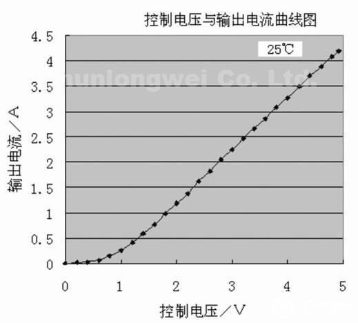
Figure 3 Constant current source control curve

System software design
The system workflow is shown in Figure 2. After power-on, the system starts self-checking. After the self-checking is completed, it enters the system initialization, including DSP, DAC, LCD, and the internal interrupt controller and counter of the DSP. After the system is ready, enter the boot Screen. Turn on the keyboard interrupt and wait for the key to select the corresponding function. If the “parameter setting” is selected, press the work key to enter the “parameter setting” interface, and you can set the voltage, current and power values. After setting, return to the startup screen and start the laser to work. After the system enters the running state, the user can still set a new value without stopping the laser. After the setting is complete, the laser will output laser according to the new requirement.
When there is an error in the system self-check and control process, or the system is over-current or over-voltage, the protection program will be called automatically. When the system is shut down or the power is suddenly cut off, in order to prevent the voltage at both ends of the laser from dropping to zero, the system adopts a full shut-down method. The principle is to gradually reduce the output of the sampled value until it drops to zero before the shutdown is allowed.
Concluding remarks
This article experimentally determines that the magnification of U1 and U2 are all 1, the output current is 0A”3A adjustable, and the laser output power is 0W”2W adjustable. The introduction of DSP control system has significantly improved compared with the previous single-chip control. Mainly manifested in: due to the high integration level and good performance of TMS320F2812, the system has the advantages of small size, fast speed, strong processing capacity, high reliability and low power consumption; the digital filtering method in TMS320F2812 is simple and the development efficiency is improved. . After the design of the driver and protection circuit of the semiconductor laser is completed, welding and debugging shall be carried out. Table 1 shows the relationship between the control voltage and the output current of the constant current source at 25°C. Figure 3 is a constant current source control curve drawn based on the data in Table 1. The output voltage range is 0V”5V, and the output current error rate is 0.1%. The output voltage and current have a linear relationship, which meets the requirements..