Using a simple probe-based solution, you can quickly identify the PDN online sensitivity, including the location of the clock jitter source.
Power distribution network (PDN) noise is one of the most common problems in low-power applications. Whether you are supplying power for ADCs, clocks, LNAs, digital data networks, or sensitive RF applications, adjusting the power supply correctly is critical. These sensitive circuits may be disturbed by power supply noise of a few millivolts or lower. Due to this extreme sensitivity and the interaction between the power supply, the distribution network and the load, it is often necessary to troubleshoot the power supply.
Due to the interaction between source impedance and load impedance, troubleshooting must be performed in the circuit, and physical access is usually very limited. As a result, this can be a time-consuming process.
Even in circuits that appear to be fully functional, the sensitivity of the power supply is usually evaluated. This is the best way to identify potential problems that may arise due to operation and environmental tolerance.
In this sample application, we will demonstrate some simple test tools that will be used in conjunction with your spectrum and network analyzer to help support power supply noise source investigations.
Figure 1 shows the Picotest VRTS3 training demo board, which includes a variety of example circuits to support multiple types of measurements.
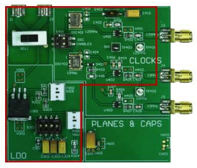
Figure 1: Picotest VRTS3 training demo board, showing the LDO and clock layout.

One of these example circuits is a 125 MHz clock (OSC401) powered by a low dropout (LDO) regulator (U301). The four-position DIP switch (S301) can be used to connect or disconnect four different output Capacitors with the LDO to change the stability of the power supply.
The schematic circuit diagram of Figure 2 shows the LDO linear regulator (LT1086), which supplies power to the 125 MHz clock oscillator OSC401 through a slide switch (SEL1). It is worth noting that the 0.01 uF decoupling capacitor C402 (on the right).
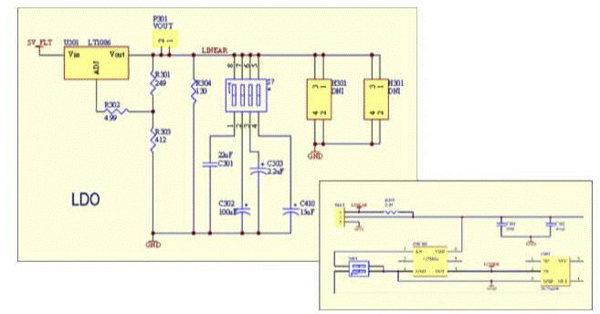
Figure 2: LDO and clock circuit

Using a broadband harmonic comb generator and a 1-port passive transmission line probe can quickly and easily realize the identification of power supply noise sensitivity.
The J2150A harmonic comb provides a broadband noise source with 50Ω output impedance. It is contained in an ultra-portable USB “stick” shape. Harmonic combs provide noise in the frequency range from 1kHz to over 1GHz in three frequency ranges. The range is centered at 1kHz, 100kHz and 8MHz. Harmonics are generated by the time and frequency jitter of the output pulse. The comb can automatically span these ranges, or it can be locked in a single frequency range. Although most instruments have several unused USB ports, the comb can also be powered by a popular cell phone backup battery to provide a portable solution.
A broadband DC module is usually included between the comb injector and the probe to isolate the 50Ω DC impedance from the circuit under test. The clock spectrum can be viewed on an oscilloscope with an optional spectrum analyzer, signal source analyzer or spectrum analyzer. The stability and distributed impedance of the voltage regulator can easily be seen as sidebands or jitter in the clock spectrum.
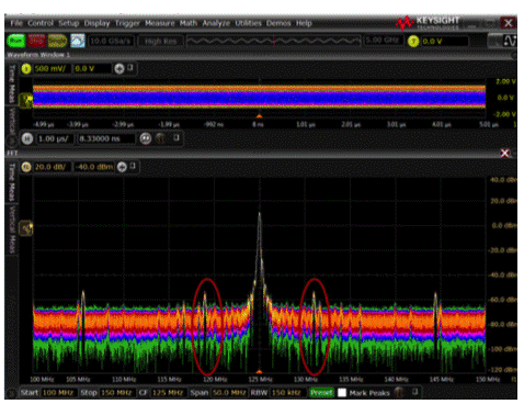
Figure 3: This oscilloscope spectrogram highlights the clock spur at approximately 6 MHz. These branches are used to demonstrate a simple and fast troubleshooting technique.

The Picotest transmission line probe is unique. It can provide unity gain and two-way 50Ω connection for various instruments through a variety of comfortable browser probes to detect power distribution networks. As shown in this example, this allows the probe to be used to inject the signal, or use the same probe to measure noise. The probe connection is a universal 50Ω SMA connector, which can be connected to most instruments.
In this example, the harmonic comb structure uses a 1-Port probe to inject broadband signals into the decoupling cap (C402) of the clock, as shown in Figure 4. Monitor the frequency spectrum of the clock on the SMA connector J3.
Figure 4: Simple but effective tool supports PDN query and clock jitter evaluation. It includes a J2150A harmonic comb broadband signal generator (left), and a 1-port (center) and 2-port bidirectional 50Ω passive probe and DC isolator (left).
Moving the noise injection point to the linear regulator (same as the printed circuit board trace, but located downstream of the clock), we noticed that at -45dBc in Figure 7, the sideband noise of the clock is much smaller. This information tells us that the resonator is between the regulator and the clock. The resonance includes the inductance of the printed circuit board traces and the decoupling capacitor C402.
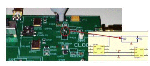
Figure 5: The J2150A harmonic comb (the inset in Figure 3) is connected to the 1-port probe through the P2130A DC blocker and used to inject the signal into the C402 (the VDD of the 125MHz clock oscillator). Monitor the clock spectrum on the SMA connector J3.

Positioning the resonance on the clock, we can use the value of the decoupling capacitor (10 nF) and the 7.5 MHz resonant frequency (7.5 MHz) to calculate the characteristic impedance of the PCB connection. The characteristic impedance can be calculated as 1/(2 * PI * 7.5 MHz * 10 nF), which is 2.1Ω in this case. Putting the SEL1 switch in the center (OFF) position will insert a 2.4Ω Resistor (R305) between the linear regulator and the clock to suppress resonance. As shown in Figure 8, the 7MHz clock spectrum sidebands are eliminated, which shows that resonance can be effectively suppressed by increasing the series resistance between the linear regulator and the clock.
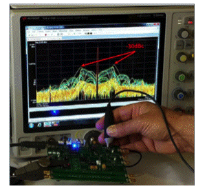
Figure 6: The PDN query using the comb search pattern signal set shows a resonance of approximately 7.5 MHz, as seen in the spectral sidebands around the fundamental frequency of the clock. Note that the peak value is approximately -30 dBc.

By using a vector network analyzer (VNA) to measure the impedance of the decoupling capacitor of the clock, resonance and damping effects can be easily confirmed. Figure 9 shows the measurement results of two different linear regulator output capacitors and the insertion of R305.
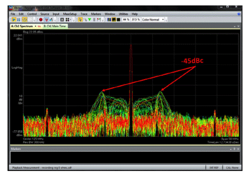
Figure 7: By injecting noise at different locations within the PDN, the noise source can be quickly located. Note that the sideband is about 15dB lower than in Figure 6. This tells us that the resonance occurs at the clock and not at the regulator.

Although the sidebands do not seem so severe, they can significantly affect performance, far more severe than other aspects. First, please note that the sideband in Figure 3 appears at 6 MHz, and we have determined that the PCB resonance is at 7.5 MHz. Second, the measurement results in Figure 9 show that at 6 MHz, the impedance is about 5 dB lower than the impedance at the 7.5 MHz peak, and at 9 MHz, the impedance is about 15 dB lower than the impedance at the 7.5 MHz peak.
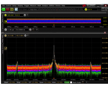
Figure 8: The 7MHz clock sideband is eliminated by inserting a series resistor between the regulator and the clock, thereby suppressing the PCB resonance.

So, what inspired the resonance? A 2.8 MHz switch point of load (POL) regulator is also provided on the VRTS3 demo board. The second and third harmonics are close enough to the resonance peak to generate clock noise. We can determine the POL switching frequency as the noise generator because an enable switch is included on the VRTS3 training board for this purpose. If the switching regulator is turned off, the 6MHz clock sideband will disappear. This also clearly explains why we are asking about the circuit, even though the circuit seems to be working properly.
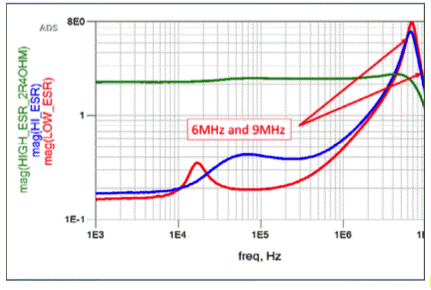
Figure 9: In two different linear regulator output capacitors (selected by switch S301), the 7.5 MHz resonance (red, blue trace) can be clearly seen. Inserting a 2.4Ω resistor can suppress resonance (green trace), thereby reducing the impedance at 7.5MHz by approximately 15 dB.

The operating frequency of the switching regulator has a tolerance of 750 kHz, and the decoupling capacitor also has a tolerance. These tolerances can easily move the second harmonic of the switching regulator to the frequency that happens to appear at the impedance peak, thereby significantly increasing clock noise. Although you are unlikely to see this frequency alignment in the nominal test, you are more likely to learn about its frequency alignment through this PDN inquiry.
All in all, we quickly determined the PDN sensitivity, which led to an increase in clock jitter. We determined the noise, determined the noise source and characteristic impedance, and easily corrected the problem by flattening the power rail impedance at the clock. Using a highly portable harmonic comb generator (Picotest J2150A), a handheld 1-port probe (Picotest P2100A) and an oscilloscope (Keysight Infiniium S), all operations can be completed in just a few minutes.
Picotest provides a variety of bundled solutions for optimizing, testing and troubleshooting power integrity issues, such as clock jitter, and supports various instruments and measurement domains. The recently launched J2150A harmonic comb generator is used in conjunction with the P2100A 1-port probe. Although it is powerful, it is only a solution.