“There are several well-known methods for dealing with power supply voltage reversal. The most obvious method is to connect a diode between the power supply and the load, but due to the forward voltage of the diode, this approach will generate additional power consumption. Although this method is very simple, the diode is not useful in portable or backup applications, because the battery must absorb current when charging and supply current when not charging.
“
Steven Martin, Battery Charger Design Manager
introduction
There are several well-known methods for dealing with power supply voltage reversal. The most obvious method is to connect a diode between the power supply and the load, but due to the forward voltage of the diode, this approach will generate additional power consumption. Although this method is very simple, the diode is not useful in portable or backup applications, because the battery must absorb current when charging and supply current when not charging.
Another method is to use one of the mosfet circuits shown in Figure 1.
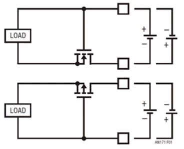
Figure 1: Traditional load-side reverse protection

For load-side circuits, this method is better than using diodes, because the power supply (battery) voltage boosts the MOSFET, resulting in less voltage drop and substantially higher conductance. The NMOS version of this circuit is better than the PMOS version because discrete NMOS transistors have higher conductivity, lower cost, and better usability. In both circuits, the MOSFET is turned on when the battery voltage is positive, and disconnected when the battery voltage is reversed. The physical “drain” of the MOSFET becomes the power source because it has a higher potential in the PMOS version and a lower potential in the NMOS version. Since mosfets are electrically symmetric in the triode region, they can conduct current well in both directions. When using this method, the Transistor must have a maximum VGS and VDS rating higher than the battery voltage.
Unfortunately, this method is only effective for load-side circuits and cannot work with circuits that can charge the battery. The battery charger will generate power, re-enable the MOSFET and re-establish the connection to the reverse battery. Figure 2 shows an example of using the NMOS version. The battery shown in the figure is in a faulty state.
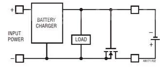
Figure 2: Load-side protection circuit with a battery charger

When the battery is connected, the battery charger is in an idle state, and the load and battery charger are safely decoupled from the reverse battery. However, if the charger changes to an operating state (for example, an input power connector is attached), the charger generates a voltage between the gate and source of the NMOS, which enhances the NMOS, thereby realizing current conduction. This is more vivid in Figure 3.

Figure 3: The traditional reverse battery protection scheme is invalid for the battery charger circuit

Although the load and charger are isolated from the reverse voltage, a major problem facing the protective MOSFET is that it consumes too much power. In this case, the battery charger becomes a battery discharger. When the battery charger provides enough gate support for the MOSFET to absorb the current delivered by the charger, the circuit will reach equilibrium. For example, if the V of a powerful MOSFETTH About 2V, and the charger can provide current under 2V voltage, the battery charger output voltage will stabilize at 2V (the drain of the MOSFET is at 2V + battery voltage). The power dissipation in the MOSFET is ICHARGE • (VTH + VBAT), so that the MOSFET heats up and generates heat until the generated heat dissipates away from the printed circuit board. The same is true for the PMOS version of this circuit.
Two alternatives to this method will be introduced below, each of which has advantages and disadvantages.
N-channel MOSFET design
The first solution uses an NMOS isolation device, as shown in Figure 4.
The algorithm of this circuit is: If the battery voltage exceeds the battery charger output voltage, the isolation MOSFET must be disabled.
As with the NMOS method described above, in this circuit, MN1 is connected to the low-voltage side of the wiring between the charger/load and the battery terminals. However, transistors MP1 and Q1 now provide a detection circuit that will deactivate MN1 in the event of a reverse battery connection. Reversing the battery raises the source of MP1 above its grid connected to the positive terminal of the charger. Then, the drain of MP1 delivers current to the base of Q1 through R1. Then, Q1 shunts the gate of MN1 to ground, preventing charging current from flowing in MN1. R1 is responsible for controlling the base current flowing to Q1 during reverse detection, while R2 provides bleeder for the base of Q1 during normal operation. R3 gives Q1 the authority to pull the gate of MN1 to ground. The R3/R4 voltage divider limits the voltage on the gate of MN1 so that the gate voltage does not have to drop that much during reverse battery hot swap. The worst case is when the battery charger is already in operation, producing its constant voltage level, and a reverse battery is attached. In this case, it is necessary to turn off MN1 as quickly as possible to limit the time when high power is consumed. This special version of the circuit with R3 and R4 is most suitable for 12V lead-acid battery applications, but in lower voltage applications such as single-cell and two-cell lithium-ion battery products, R4 can be exempted. Capacitor C1 provides an ultra-fast charge pump to pull down the gate level of MN1 during reverse battery attachment. For the worst case (when a reverse battery is attached, the charger has been enabled again), C1 is very useful.
The disadvantage of this circuit is that additional components are required. The R3/R4 voltage divider creates a small but continuous load on the battery.
Most of these components are slim. MP1 and Q1 are not power devices, and usually SOT23-3, SC70-3 or smaller packages are available. MN1 should have very good conductivity, because it is a transmission device, but the size does not have to be large. Because it works in the deep triode region and has been greatly strengthened by the gate, its power consumption is very low even for devices with medium conductivity. For example, transistors below 100mΩ are often packaged in SOT23-3.
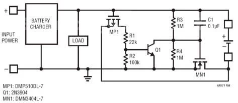
Figure 4: A feasible reverse battery circuit

However, the disadvantage of using a small pass Transistor is that the additional impedance in series with the battery charger extends the charging time during the constant voltage charging phase. For example, if the battery and its wiring have an equivalent series resistance of 100mΩ, and a 100mΩ isolation transistor is used, the charging time during the constant voltage charging phase will be doubled.
The detection and deactivation circuit composed of MP1 and Q1 is not particularly fast to deactivate MN1, and they do not need to be so. Although MN1 generates high power consumption during reverse battery attachment, the shutdown circuit only needs to disconnect MN1 “at the end”. It must disconnect MN1 before MN1 heats up so much that it causes damage. A disconnection time of tens of microseconds may be more suitable. On the other hand, it is critical to disable MN1 before the reverse connection of the battery has the opportunity to pull the charger and load voltage to a negative value, so C1 is required. Basically, the circuit has one AC and one DC deactivation path.
This circuit was tested with a lead-acid battery and LTC4015 battery charger. As shown in Figure 5, the battery charger is in the OFF state when the battery is hot-plugged in the reverse direction. The reverse voltage will not be transmitted to the charger and load.
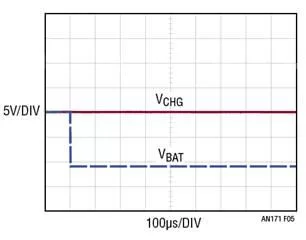
Figure 5: NMOS protection circuit with the charger in the off state

It is worth noting that MN1 needs a V equal to the battery voltageDS Rated value and a V equal to 1/2 battery voltageGS Rated value. MP1 needs a V equal to the battery voltageDS And VGS Rated value.
Figure 6 shows a more serious situation, that is, the battery charger is already in normal operation when the reverse battery is hot-swapped. Reverse connection of the battery will pull down the charger side voltage until the detection and protection circuit makes it out of operation, allowing the charger to safely return to its constant voltage level. The dynamic characteristics will vary from application to application, and the capacitance on the battery charger will play a big role in the final result. In this test, the battery charger has both a high-Q ceramic capacitor and a low-Q polymer capacitor.
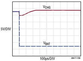
Figure 6: NMOS protection circuit with the charger in operation

In short, it is recommended to use aluminum polymer Capacitors and aluminum electrolytic capacitors on the battery charger to improve the performance during normal positive battery hot-plugging. Due to the extreme non-linearity, pure ceramic capacitors will produce excessive overshoot during hot plugging. The reason behind this is that when the voltage rises from 0V to the rated voltage, the capacitance decreases by an astonishing 80%. This non-linearity stimulates the flow of high current under low voltage conditions, and when the voltage rises, the capacitance decreases rapidly; this is a lethal combination that causes a very high voltage overshoot. As a rule of thumb, the combination of a ceramic capacitor and a low-Q, voltage-stable aluminum capacitor or even a tantalum capacitor seems to be the most robust combination.
P-channel MOSFET design
Figure 7 shows the second method, which uses a PMOS transistor as a protection device.

Figure 7: PMOS transistor transmission element version

In this circuit, MP1 is a reverse battery detection device, and MP2 is a reverse isolation device. Use the source-to-gate voltage of MP1 to compare the positive terminal of the battery with the battery charger output. If the battery charger terminal voltage is higher than the battery voltage, MP1 will deactivate the main transmission device MP2. Therefore, if the battery voltage is driven below ground, it is clear that the detection device MP1 will drive the transmission device MP2 to the off state (interfering its gate to its source). Regardless of whether the battery charger is enabled and forms a charging voltage or disabled (0V), it will complete the above operations.
The biggest advantage of this circuit is that the PMOS isolation transistor MP2 does not have the authority to transmit the negative voltage to the charger circuit and the load. Figure 8 illustrates this more clearly.
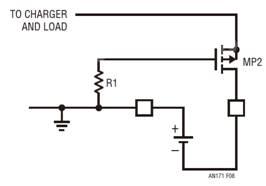
Figure 8: Diagram of cascode effect

The lowest voltage that can be achieved on the gate of MP2 through R1 is 0V. Even if the drain of MP2 is pulled far below ground potential, its source will not apply significant voltage downward pressure. Once the source voltage drops to V where the transistor is above groundTH, The transistor will release its own bias, and its conductivity will gradually disappear. The closer the source voltage is to the ground potential, the higher the degree of bias release of the transistor. This feature, coupled with the simple topology, makes this method more popular than the NMOS method described above. Compared with the NMOS method, it does have the disadvantages of lower conductivity and higher cost of PMOS transistors.
Although simpler than the NMOS method, this circuit has a big disadvantage. Although it always provides protection against reverse voltage, it may not always connect the circuit to the battery. When the gate is cross-coupled as shown in the figure, the circuit forms a latched storage element, which may choose the wrong state. Although it is difficult to achieve, there is a situation in which the charger is generating a voltage (for example, 12V), and when a battery is attached at a lower voltage (for example, 8V), the circuit is disconnected.
In this case, the source-to-gate voltage of MP1 is +4V, thus strengthening MP1 and deactivating MP2. This situation is shown in Figure 9 and a stable voltage is listed on the node.

Figure 9: Diagram of possible blocking states when using PMOS protection circuit

In order to achieve this condition, the charger must already be running when the battery is connected. If the battery is connected before the charger is enabled, the gate voltage of MP1 is completely pulled up by the battery, thus disabling MP1. When the charger is switched on, it generates a controlled current (rather than a high current surge), which reduces the possibility of MP1 being switched on and MP2 being switched off.
On the other hand, if the charger is enabled before the battery is attached, the gate of MP1 simply follows the battery charger output because it is pulled up by the bleeder Resistor R2. When the battery is not connected, MP1 has no tendency to turn on and make MP2 out of operation.
When the charger is up and running, and the battery is attached, a problem occurs. In this case, there is a momentary difference between the charger output and the battery terminals, which will cause MP1 to take MP2 out of operation, because the battery voltage forces the charger capacitor to absorb. This creates a competition between MP2’s ability to draw charge from the charger capacitor and MP1’s ability to take MP2 out of operation.
The circuit was also tested with a lead-acid battery and LTC4015 battery charger. Connecting a heavy-loaded 6V power supply as a battery simulator to an enabled battery charger will never trigger the “disconnected” state. The tests done are not comprehensive and should be tested more comprehensively and thoroughly in key applications. Even if the circuit is indeed locked, disabling the battery charger and re-enabling it will always result in a reconnection.
The fault state can be demonstrated by manipulating the circuit (establishing a temporary connection between the top of R1 and the battery charger output). However, it is generally believed that the circuit is more inclined to be connected. If connection failure does become a problem, you can design a circuit that uses multiple devices to disable the battery charger. Figure 12 shows a more complete circuit example.
Figure 10 shows the effect of the PMOS protection circuit with the charger disabled.
Please note that no matter what the situation is, there will be no negative voltage transfer between the battery charger and the load voltage.
Figure 11 shows that the circuit is in the unfavorable situation of “the charger has entered the operating state when the battery is reversely connected for hot plugging”.
The effect of the NMOS circuit is almost the same. Before disconnecting the circuit to make the transfer transistor MP2 out of operation, the reverse battery slightly pulls down the charger and load voltage.
In this version of the circuit, the transistor MP2 must be able to withstand twice the voltage of the battery VDS (One for the charger and one for the reverse connection of the battery) and V equal to the battery voltageGS. On the other hand, MP1 must be able to withstand V equal to the battery voltageDSAnd V which is twice the battery voltageGS. This requirement is regrettable, because for MOSFET transistors, the rated VDSAlways exceed rated VGS. Can be found with 30V VGS Tolerance and 40V VDS Tolerant transistors are suitable for lead-acid battery applications. In order to support higher voltage batteries, Zener diodes and current limiting resistors must be added to modify the circuit.
Figure 12 shows an example of a circuit that can handle two lead-acid batteries stacked in series.

Figure 10: PMOS protection circuit with the charger in the off state

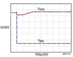
Figure 11: PMOS protection circuit with the charger in operation

ADI believes that the information it provides is accurate and reliable. However, ADI is not responsible for its use and any infringement of third-party patents or other rights that may result from its use. Specifications are subject to change without notice. No license to use any patents or patent rights of ADI shall be granted by implication or otherwise.
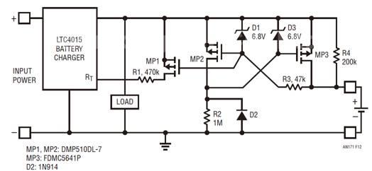
Figure 12: Higher voltage reverse battery protection.

D1, D3 and R3 protect the gates of MP2 and MP3 from high voltage damage. When a reversed battery is hot swapped, D2 can prevent the MP3 grid and battery charger output from quickly moving below ground potential. When the circuit has a reverse battery or is in a wrong disconnection lockout state, MP1 and R1 can be detected, and use the missing RT feature of LTC4015 to disable the battery charger.
in conclusion
It is possible to develop a reverse voltage protection circuit for battery charger-based applications. People have developed some circuits and conducted brief tests, and the test results are encouraging. There is no clever trick for the reverse battery problem, but I hope that the method introduced in this article can provide sufficient enlightenment, that is, there is a simple, low-cost solution.
Steven Martin, battery charger design manager
introduction
There are several well-known methods for dealing with power supply voltage reversal. The most obvious method is to connect a diode between the power supply and the load, but due to the forward voltage of the diode, this approach will generate additional power consumption. Although this method is very simple, the diode is not useful in portable or backup applications, because the battery must absorb current when charging and supply current when not charging.
Another method is to use one of the MOSFET circuits shown in Figure 1.
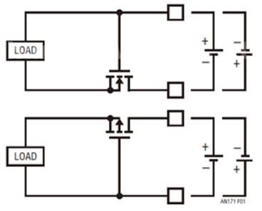
Figure 1: Traditional load-side reverse protection
For load-side circuits, this method is better than using diodes, because the power supply (battery) voltage boosts the MOSFET, resulting in less voltage drop and substantially higher conductance. The NMOS version of this circuit is better than the PMOS version because discrete NMOS transistors have higher conductivity, lower cost, and better usability. In both circuits, the MOSFET is turned on when the battery voltage is positive, and disconnected when the battery voltage is reversed. The physical “drain” of the MOSFET becomes the power source because it has a higher potential in the PMOS version and a lower potential in the NMOS version. Since MOSFETs are electrically symmetrical in the triode region, they can conduct current well in both directions. When using this method, the transistor must have a maximum VGS and VDS rating higher than the battery voltage.
Unfortunately, this method is only effective for load-side circuits and cannot work with circuits that can charge the battery. The battery charger will generate power, re-enable the MOSFET and re-establish the connection to the reverse battery. Figure 2 shows an example of using the NMOS version. The battery shown in the figure is in a faulty state.

Figure 2: Load-side protection circuit with a battery charger
When the battery is connected, the battery charger is in an idle state, and the load and battery charger are safely decoupled from the reverse battery. However, if the charger changes to an operating state (for example, an input power connector is attached), the charger generates a voltage between the gate and source of the NMOS, which enhances the NMOS, thereby realizing current conduction. This is more vivid in Figure 3.
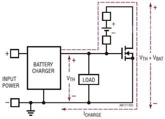
Figure 3: The traditional reverse battery protection scheme is invalid for the battery charger circuit
Although the load and charger are isolated from the reverse voltage, a major problem facing the protective MOSFET is that it consumes too much power. In this case, the battery charger becomes a battery discharger. When the battery charger provides enough gate support for the MOSFET to absorb the current delivered by the charger, the circuit will reach equilibrium. For example, if the V of a powerful MOSFETTH About 2V, and the charger can provide current under 2V voltage, the battery charger output voltage will stabilize at 2V (the drain of the MOSFET is at 2V + battery voltage). The power dissipation in the MOSFET is ICHARGE • (VTH + VBAT), so that the MOSFET heats up and generates heat until the generated heat dissipates away from the printed circuit board. The same is true for the PMOS version of this circuit.
Two alternatives to this method will be introduced below, each of which has advantages and disadvantages.
N-channel MOSFET design
The first solution uses an NMOS isolation device, as shown in Figure 4.
The algorithm of this circuit is: If the battery voltage exceeds the battery charger output voltage, the isolation MOSFET must be disabled.
As with the NMOS method described above, in this circuit, MN1 is connected to the low-voltage side of the wiring between the charger/load and the battery terminals. However, transistors MP1 and Q1 now provide a detection circuit that will deactivate MN1 in the event of a reverse battery connection. Reversing the battery raises the source of MP1 above its grid connected to the positive terminal of the charger. Then, the drain of MP1 delivers current to the base of Q1 through R1. Then, Q1 shunts the gate of MN1 to ground, preventing charging current from flowing in MN1. R1 is responsible for controlling the base current flowing to Q1 during reverse detection, while R2 provides bleeder for the base of Q1 during normal operation. R3 gives Q1 the authority to pull the gate of MN1 to ground. The R3/R4 voltage divider limits the voltage on the gate of MN1 so that the gate voltage does not have to drop that much during reverse battery hot swap. The worst case is when the battery charger is already in operation, generating its constant voltage level, and a reverse battery is attached. In this case, it is necessary to turn off MN1 as quickly as possible to limit the time when high power is consumed. This special version of the circuit with R3 and R4 is most suitable for 12V lead-acid battery applications, but in lower voltage applications such as single-cell and two-cell lithium-ion battery products, R4 can be exempted. Capacitor C1 provides an ultra-fast charge pump to pull down the gate level of MN1 during reverse battery attachment. For the worst case (when a reverse battery is attached, the charger has been enabled again), C1 is very useful.
The disadvantage of this circuit is that additional components are required. The R3/R4 voltage divider creates a small but continuous load on the battery.
Most of these components are slim. MP1 and Q1 are not power devices, and usually SOT23-3, SC70-3 or smaller packages are available. MN1 should have very good conductivity because it is a transmission device, but it does not have to be large in size. Because it works in the deep triode region and has been greatly strengthened by the gate, its power consumption is very low even for devices with medium conductivity. For example, transistors below 100mΩ are often packaged in SOT23-3.

Figure 4: A feasible reverse battery circuit
However, the disadvantage of using a small pass transistor is that the additional impedance in series with the battery charger extends the charging time during the constant voltage charging phase. For example, if the battery and its wiring have an equivalent series resistance of 100mΩ, and a 100mΩ isolation transistor is used, the charging time during the constant voltage charging phase will be doubled.
The detection and deactivation circuit composed of MP1 and Q1 is not particularly fast to deactivate MN1, and they do not need to be so. Although MN1 generates high power consumption during reverse battery attachment, the shutdown circuit only needs to disconnect MN1 “at the end”. It must disconnect MN1 before MN1 heats up so much that it causes damage. A disconnection time of tens of microseconds may be more suitable. On the other hand, it is critical to disable MN1 before the reverse connection of the battery has the opportunity to pull the charger and load voltage to a negative value, so C1 is required. Basically, the circuit has one AC and one DC deactivation path.
This circuit was tested with a lead-acid battery and LTC4015 battery charger. As shown in Figure 5, the battery charger is in the OFF state when the battery is hot-plugged in the reverse direction. The reverse voltage will not be transmitted to the charger and load.

Figure 5: NMOS protection circuit with the charger in the off state
It is worth noting that MN1 needs a V equal to the battery voltageDS Rated value and a V equal to 1/2 battery voltageGS Rated value. MP1 needs a V equal to the battery voltageDS And VGS Rated value.
Figure 6 shows a more serious situation, that is, the battery charger is already in normal operation when the reverse battery is hot-swapped. Reverse connection of the battery will pull down the voltage on the charger side until the detection and protection circuit makes it out of operation, allowing the charger to safely return to its constant voltage level. The dynamic characteristics will vary from application to application, and the capacitance on the battery charger will play a big role in the final result. In this test, the battery charger has both a high-Q ceramic capacitor and a low-Q polymer capacitor.

Figure 6: NMOS protection circuit with the charger in operation
In short, it is recommended to use aluminum polymer capacitors and aluminum electrolytic capacitors on the battery charger to improve the performance during normal positive battery hot-plugging. Due to the extreme non-linearity, pure ceramic capacitors will produce excessive overshoot during hot plugging. The reason behind this is that when the voltage rises from 0V to the rated voltage, the capacitance decreases by an astonishing 80%. This non-linearity stimulates the flow of high currents under low voltage conditions, and when the voltage rises, the capacitance decreases rapidly; this is a lethal combination that leads to very high voltage overshoots. As a rule of thumb, the combination of a ceramic capacitor and a low-Q, voltage-stable aluminum capacitor or even a tantalum capacitor seems to be the most robust combination.
P-channel MOSFET design
Figure 7 shows the second method, which uses a PMOS transistor as a protection device.
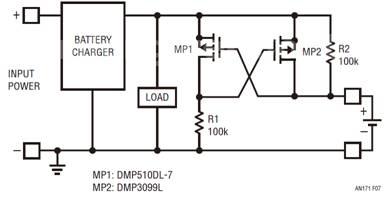
Figure 7: PMOS transistor transmission element version
In this circuit, MP1 is a reverse battery detection device, and MP2 is a reverse isolation device. Use the source-to-gate voltage of MP1 to compare the positive terminal of the battery with the battery charger output. If the battery charger terminal voltage is higher than the battery voltage, MP1 will deactivate the main transmission device MP2. Therefore, if the battery voltage is driven below ground, it is clear that the detection device MP1 will drive the transmission device MP2 to the off state (interfering its gate to its source). Regardless of whether the battery charger is enabled and forms a charging voltage or disabled (0V), it will complete the above operations.
The biggest advantage of this circuit is that the PMOS isolation transistor MP2 does not have the authority to transmit the negative voltage to the charger circuit and the load. Figure 8 illustrates this more clearly.

Figure 8: Diagram of the cascode effect
The lowest voltage that can be achieved on the gate of MP2 through R1 is 0V. Even if the drain of MP2 is pulled far below ground potential, its source will not apply significant voltage downward pressure. Once the source voltage drops to V where the transistor is above groundTH, The transistor will release its own bias and its conductivity will gradually disappear. The closer the source voltage is to the ground potential, the higher the degree of bias release of the transistor. This feature, coupled with the simple topology, makes this method more popular than the NMOS method described above. Compared with the NMOS method, it does have the disadvantages of lower conductivity and higher cost of PMOS transistors.
Although simpler than the NMOS method, this circuit has a big disadvantage. Although it always provides protection against reverse voltage, it may not always connect the circuit to the battery. When the gates are cross-coupled as shown, the circuit forms a latched storage element, which may choose the wrong state. Although it is difficult to achieve, there is a situation in which the charger is generating a voltage (for example, 12V), and when a battery is attached at a lower voltage (for example, 8V), the circuit is disconnected.
In this case, the source-to-gate voltage of MP1 is +4V, thus strengthening MP1 and deactivating MP2. This situation is shown in Figure 9 and a stable voltage is listed on the node.
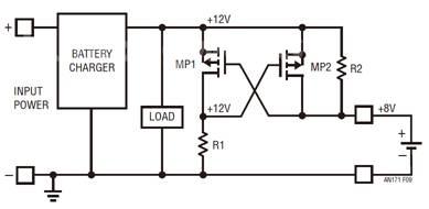
Figure 9: Diagram of possible blocking states when using PMOS protection circuit
In order to achieve this condition, the charger must already be running when the battery is connected. If the battery is connected before the charger is enabled, the gate voltage of MP1 is completely pulled up by the battery, thus disabling MP1. When the charger is switched on, it generates a controlled current (rather than a high current surge), which reduces the possibility of MP1 being switched on and MP2 being switched off.
On the other hand, if the charger is enabled before the battery is attached, the gate of MP1 simply follows the battery charger output because it is pulled up by the bleeder resistor R2. When the battery is not connected, MP1 has no tendency to turn on and make MP2 out of operation.
When the charger is up and running, and the battery is attached, a problem occurs. In this case, there is a momentary difference between the charger output and the battery terminals, which will cause MP1 to take MP2 out of operation, because the battery voltage forces the charger capacitor to absorb. This creates a competition between MP2’s ability to draw charge from the charger capacitor and MP1’s ability to take MP2 out of operation.
The circuit was also tested with a lead-acid battery and LTC4015 battery charger. Connecting a heavy-loaded 6V power supply as a battery simulator to an enabled battery charger will never trigger the “disconnected” state. The tests done are not comprehensive and should be tested more comprehensively and thoroughly in key applications. Even if the circuit is indeed locked, disabling the battery charger and re-enabling it will always result in a reconnection.
The fault state can be demonstrated by manipulating the circuit (establishing a temporary connection between the top of R1 and the battery charger output). However, it is generally believed that the circuit is more inclined to be connected. If connection failure does become a problem, you can design a circuit that uses multiple devices to disable the battery charger. Figure 12 shows a more complete circuit example.
Figure 10 shows the effect of the PMOS protection circuit with the charger disabled.
Please note that no matter what the situation is, there will be no negative voltage transfer between the battery charger and the load voltage.
Figure 11 shows that the circuit is in the unfavorable situation of “the charger has entered the operating state when the battery is reversely connected for hot plugging.”
The effect of the NMOS circuit is almost the same. Before disconnecting the circuit to make the transfer transistor MP2 out of operation, the reverse battery slightly pulls down the charger and load voltage.
In this version of the circuit, the transistor MP2 must be able to withstand twice the voltage of the battery VDS (One for the charger and one for the reverse connection of the battery) and V equal to the battery voltageGS. On the other hand, MP1 must be able to withstand V equal to the battery voltageDSAnd V which is twice the battery voltageGS. This requirement is regrettable, because for MOSFET transistors, the rated VDSAlways exceed rated VGS. Can be found with 30V VGS Tolerance and 40V VDS Tolerant transistors are suitable for lead-acid battery applications. In order to support higher voltage batteries, Zener diodes and current limiting resistors must be added to modify the circuit.
Figure 12 shows an example of a circuit that can handle two lead-acid batteries stacked in series.
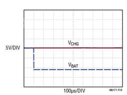
Figure 10: PMOS protection circuit with the charger in the off state

Figure 11: PMOS protection circuit with the charger in operation
ADI believes that the information it provides is accurate and reliable. However, ADI is not responsible for its use and any infringement of third-party patents or other rights that may result from its use. Specifications are subject to change without notice. No license to use any patents or patent rights of ADI shall be granted by implication or otherwise.

Figure 12: Higher voltage reverse battery protection.
D1, D3 and R3 protect the gates of MP2 and MP3 from high voltage damage. When a reversed battery is hot swapped, D2 can prevent the MP3 grid and battery charger output from quickly moving below ground potential. When the circuit has a reverse battery or is in a wrong disconnection lockout state, MP1 and R1 can be detected, and use the missing RT feature of LTC4015 to disable the battery charger.
in conclusion
A reverse voltage protection circuit for battery charger-based applications can be developed. People have developed some circuits and conducted brief tests, and the test results are encouraging. There is no clever trick for the reverse battery problem, but I hope that the method introduced in this article can provide sufficient enlightenment, that is, there is a simple, low-cost solution.
The Links: NL6448BC33-59D FS450R12KE3