BF300R12KS4 1200V 300A Dual IGBT Module: Technical Specification and Application Guide
BF300R12KS4 | 1200V 300A Dual IGBT Module Specification
Introduction & Core Highlights
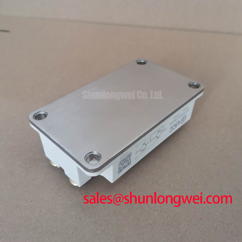
The BF300R12KS4 is a high-speed, half-bridge dual IGBT Module rated for 1200V and 300A, designed to optimize power density in high-frequency converter topologies. Housed in a industry-standard 62mm package, this module is engineered to minimize switching energy losses during high-speed transitions. This makes it a robust alternative for hard-switching applications operating in ranges where conventional components face thermal limitations.
- Core Specifications: 1200V Collector-Emitter Voltage | 300A Continuous Collector Current (at Tc = 80°C) | High-Speed Switching Technology
- Key Benefits: Reduced switching losses lower cooling assembly footprint; standardized 62mm layout simplifies mechanical integration.
- Design Intention: For engineers asking how switching losses scale with frequency in fast-switching 1200V modules, the BF300R12KS4 features optimized carrier lifetime control to maintain low thermal dissipation above 15 kHz.
Download Official Datasheet (PDF)


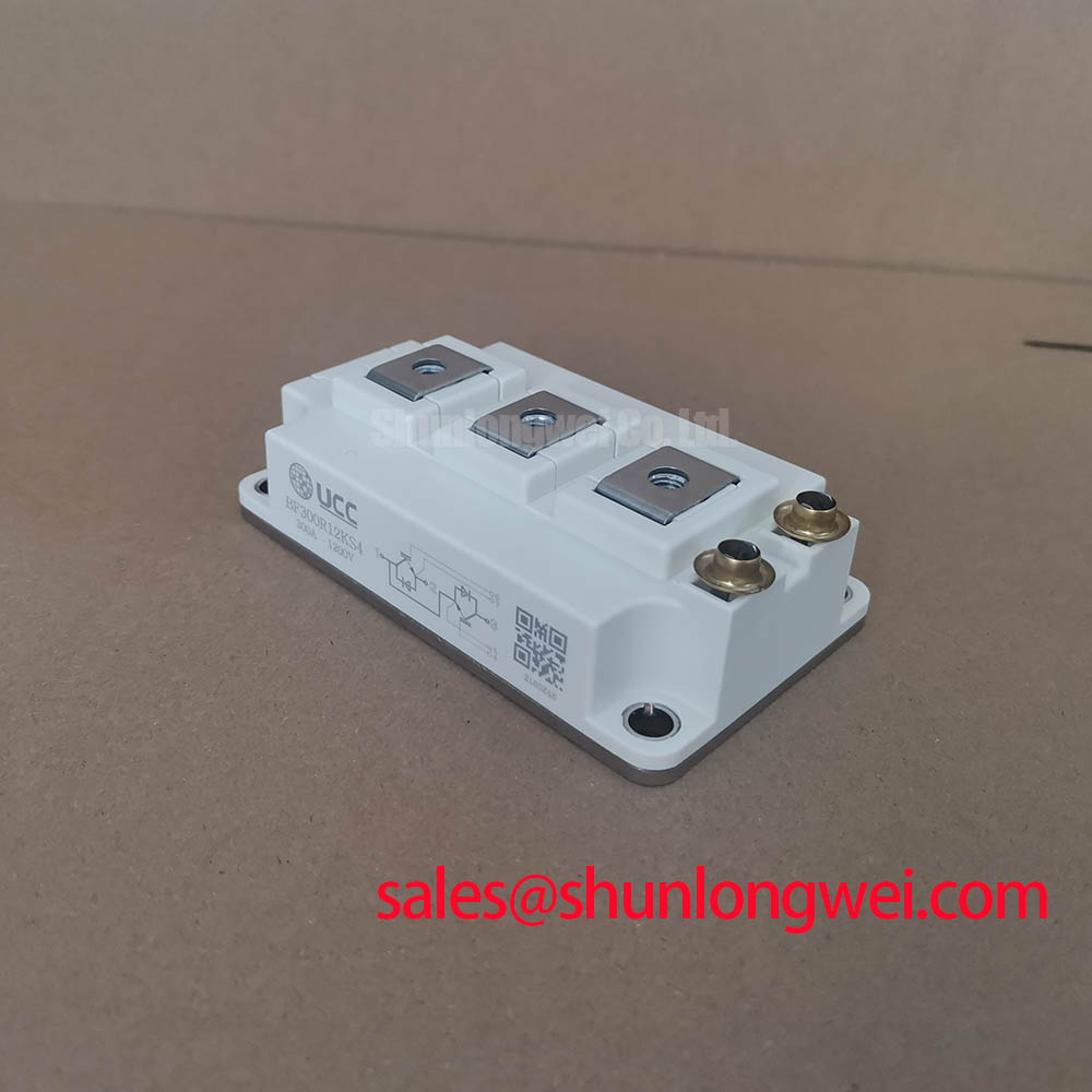
Technical Analysis of the BF300R12KS4
The primary advantage of the BF300R12KS4 lies in its switching performance. In high-frequency converters, switching losses typically dominate the total thermal dissipation profile. The module addresses this by utilizing a carrier lifetime-killing process. This process accelerates the recombination of minority carriers inside the drift region when the gate voltage goes low, significantly curtailing the turn-off tail current.
To understand this switching dynamics, imagine a sponge representing the semiconductor drift region. A standard low-conduction IGBT acts like a dense sponge that holds water tightly. It conducts current efficiently but takes a long time to squeeze dry during turn-off, creating a prolonged tail current. The high-speed BF300R12KS4 behaves like a highly porous sponge. It releases its charge carriers almost instantly during turn-off, preventing switching energy build-up at high operating frequencies.
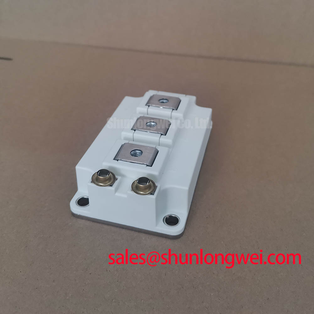
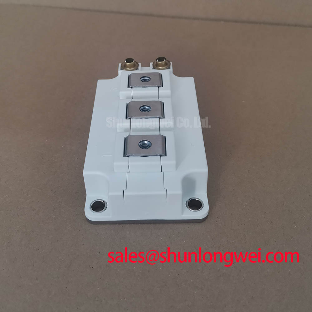
Because the turn-off transition is rapid, managing circuit path parasitics becomes crucial. High rates of current change ($di/dt$) interact with circuit inductances, producing voltage overshoots. Proper layout design must prioritize low-induction busbars to prevent exceeding the 1200V rating. Engineers must evaluate the parasitic inductance of the gate loop and implement precise gate resistor selection to balance switching speed with electromagnetic compatibility.
Optimized Application Scenarios
- Solar Inverters: The high-speed switching capabilities enable the use of smaller inductors and output filters, raising the overall power density of the inverter system.
- High-Frequency Induction Heating: Low turn-off losses allow resonant topologies to operate reliably at higher frequencies, reducing package thermal stress.
- Uninterruptible Power Supplies (UPS): The half-bridge configuration simplifies layout design in online double-conversion UPS systems, ensuring stable output wave generation.
- Industrial Welding Power Supplies: The module supports rapid transient responses, stabilizing output welding currents under highly dynamic load variations.
Best Match: The BF300R12KS4 is ideal for hard-switching inverter topologies operating in the 10 kHz to 30 kHz range where thermal dissipation limits traditional IGBTs.
Key Specifications Table
| Absolute Maximum Ratings | |
|---|---|
| Collector-Emitter Voltage ($V_{CES}$) | 1200 V (at $T_vj = 25^circ C$) |
| Continuous DC Collector Current ($I_C$) | 300 A (at $T_C = 80^circ C$) |
| Repetitive Peak Collector Current ($I_{CRM}$) | 600 A (for $t_p = 1 ms$) |
| Gate-Emitter Peak Voltage ($V_{GES}$) | ±20 V |
| Electrical Characteristics (IGBT) | |
| Collector-Emitter Saturation Voltage ($V_{CE(sat)}$) | 3.20 V (typical, at $I_C = 300A, T_{vj} = 125^circ C$) |
| Gate Threshold Voltage ($V_{GE(th)}$) | 4.5 V to 6.5 V (typical 5.8 V at $I_C = 12 mA, V_{CE} = V_{GE}$) |
| Input Capacitance ($C_{ies}$) | 21 nF (typical, at $f = 1 MHz, V_{CE} = 25V, V_{GE} = 0V$) |
| Thermal and Mechanical Characteristics | |
| Thermal Resistance, Junction to Case ($R_{thJC}$) | 0.085 K/W (typical, per IGBT) |
| Isolation Test Voltage ($V_{ISOL}$) | 2.5 kV (AC, 1 minute, $f = 50 Hz$) |
| Mounting Torque (M5 / M6 Screws) | Mounting: 3.0 to 6.0 Nm | Terminal Connection: 2.5 to 5.0 Nm |
Engineer FAQ
How do switching losses scale with frequency in the BF300R12KS4?
Due to the short carrier lifetime design, the turn-off tail current is minimal. While conduction losses ($V_{CE(sat)}$) are higher than standard switching frequency modules, switching losses scale linearly with a much lower slope, making this module suitable for frequencies up to 30 kHz under appropriate cooling conditions.
What is the structure and benefit of the isolated baseplate in this module?
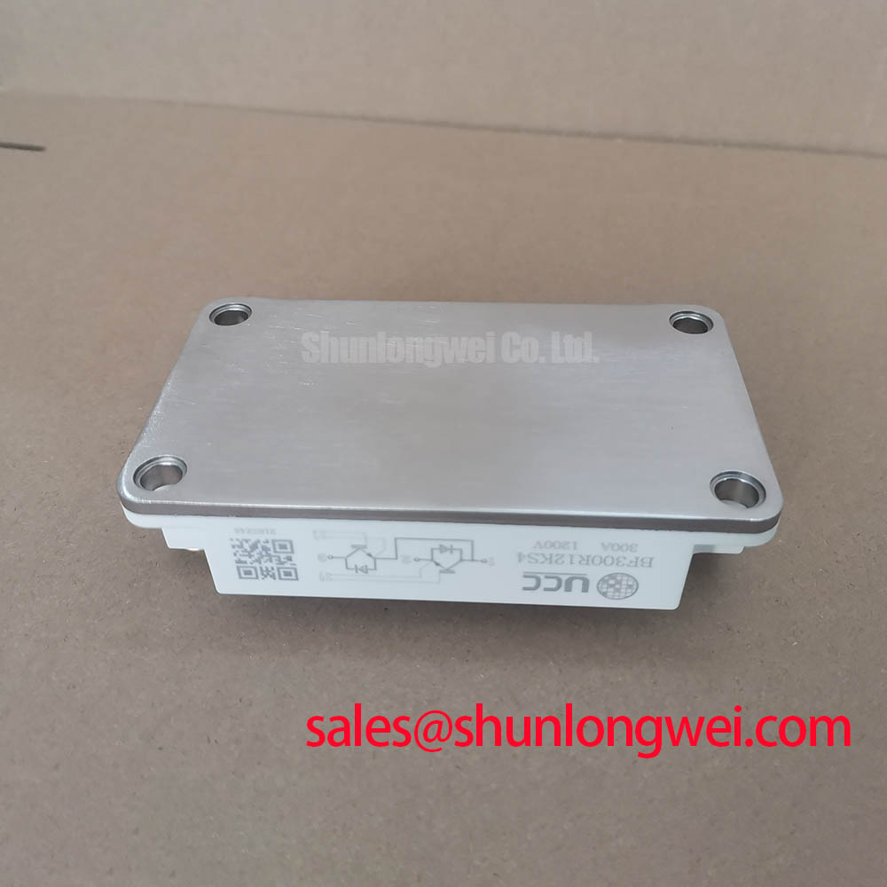
The module is constructed on isolated baseplates using direct copper bonding (DCB) ceramic substrates. This layout isolates the electrical connections from the metal heatsink, facilitating the mounting of multiple modules on a single thermal block without individual isolation pads.
What gate driver protections are recommended for this package?
A gate drive circuit providing active miller clamp protection is recommended to prevent parasitic turn-on caused by high $dV/dt$ transients. Desaturation ($V_{CE}$) sensing must be configured to shut down the gate drive gracefully during overcurrent events, avoiding stress spikes on the chip.
Closing Statement
The BF300R12KS4 provides a balanced solution for power designers seeking high-frequency operation within standard 62mm form factors. By lowering turn-off energy dissipation, this module supports high-speed switching targets while maintaining standard mechanical interfaces. Integrating this component into your layout helps scale switching frequency limits while preserving power conversion efficiency.