Advanced packaging market to be worth $47.5bn in 2026, says Yole
The share of advanced packaging in the total Semiconductor market is increasing continuously and expected to reach almost 50% of the market by 2026.
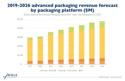
The highest revenue CAGRs are expected from 3D stacking, ED and Fan-Out, at 22%, 25% and 15% respectively between 2020 and 2026.
Heterogeneous integration is seen to increase the value of a semiconductor product, adding functionality, maintaining/increasing performance while lowering cost.
A variety of multi-die packaging (SiP ) is being developed in both high and low end, for consumer, performance, and specialized applications.
The semiconductor manufacturing supply chain is undergoing change at various levels. IC substrate & PCB manufacturers, such as SEMCO, Unimicron, AT&S and Shinko, are entering the advanced packaging area. OSATs are expanding their testing expertise, while traditional pure test players are investing in assembly /packaging capabilities. TSMC, Intel & Samsung have emerged as the key innovators of new advanced packaging technology.
“The advanced packaging market was worth $30 billion in 2020 and is expected to grow at a CAGR of 8% to reach $47.5 billion in 2026 during this period” says Yole’s Santosh Kumar “at the same time, the traditional packaging market will grow at a 4.3% CAGR to reach US$50 billion in 2026. In this context, the total packaging market is showing a 6% CAGR with a US$95.4 billion value the same year.”
Flip-chip constitutes about 80% of the advanced packaging market in 2020 and will continue to command a significant portion (almost 72%) of the market by 2026.
Of the different advanced packaging platforms, 3D/2.5D stacking and fan-out will grow at about 22% and 16%, respectively. Adoption will continue to increase across various applications.
Mainly led by mobile, Fan-In WLP (WLCSP ) will grow at a CAGR of 5% between 2020 and 2026.
Though small (almost $51 million in 2020), the embedded die market is expected to grow at a 22% CAGR in the next 5 years, with demand driven by the telecom & infrastructure, automotive & mobile markets.
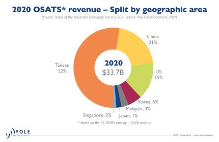
OSATs currently dominate the advanced packaging market. OSATs account for about 70% of the total market by wafer starts. However, in the high end of the packaging segment, including 2.5D/3D stacking, high-density Fan-Out, the big foundries, like TSMC, and IDM s, like Intel and Samsung, dominate the market.
These players are investing heavily in advanced packaging technology. They are instrumental in moving packaging from substrate to wafer /silicon platforms. Stefan Chitoraga, Technology & Market Analyst at Yole comments: “TSMC earned about $3.6 billion in advanced packaging revenue in 2020. The company announced an estimated $2.8 billion CapEx in 2021 for its advanced packaging business specifically geared towards SoIC, SoW, and InFO variants, and CoWoS product lines. In parallel, Intel’s investment in various advanced packaging portfolios, such as Foveros, EMIB, Co-EMIB, is key to implement its IDM 2.0 strategy as unveiled by new leadership. They plan to capitalize on external and internal manufacturing resources to focus on design wins and increased market share, growing Intel’s leadership in the client and data center domains”.
From its side, Samsung is aggressively investing in advanced packaging technology to boost its foundry business and emerge as a strong alternative to TSMC. On the other hand, OSATs are also investing heavily in advanced packaging technologies to compete in the lucrative market.
OSATs’ CapEx spending increased 27% YoY in 2020. It represents about US$6 billion. This strategy contributed to the very good financial year despite the COVID-19 impact.
Overall, there is a paradigm shift in the packaging / assembly business, traditionally the domain of OSATs and IDMs. Players from different business models including foundries, substrate/PCB suppliers, EMS/DM , are entering the assembly/ packaging business.