Of course. Here is the provided technical review, formatted as a complete and well-structured HTML page.
“`html
IXFN180N10 N-Channel Power MOSFET: 100V, 180A Performance
IXFN180N10 N-Channel Power MOSFET: 100V, 180A Performance
Introduction to the IXFN180N10 HiPerFET™ Power MOSFET
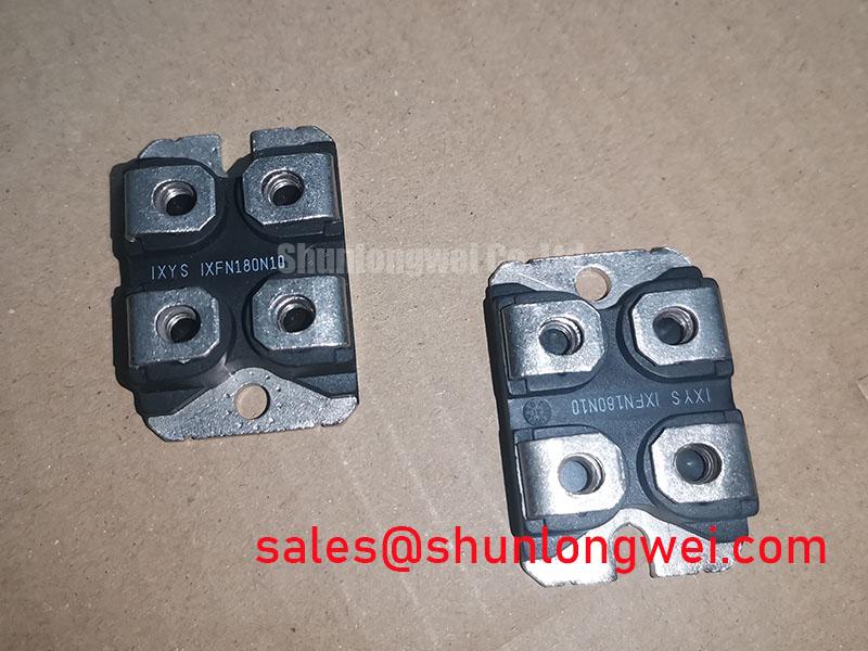
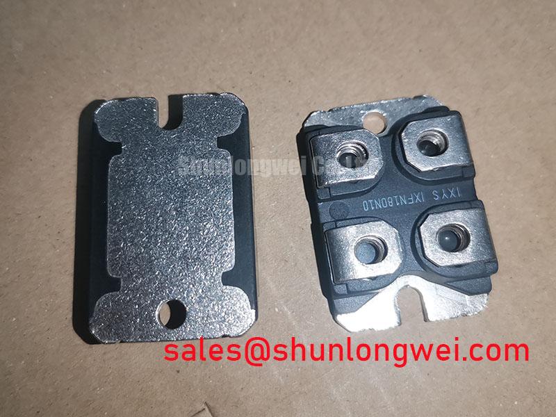
The IXFN180N10 is an N-Channel enhancement mode Power MOSFET engineered for high-power switching applications. Its primary value stems from combining a high continuous drain current rating with the mounting convenience and electrical isolation of the SOT-227 (miniBLOC) package. This structure provides a straightforward path for thermal management while handling substantial power, addressing a common challenge for engineers designing compact systems.
- Core Specifications: 100V | 180A | 7.0 mΩ RDS(on)
- Key Advantages: Simplified assembly with an isolated package; low conduction losses for improved system efficiency.
For complete specifications and performance graphs, download the official IXFN180N10 datasheet (PDF).

Technical Analysis of Core Features
A detailed review of the datasheet reveals several parameters that directly influence system design. The most prominent is the SOT-227 package, which features an aluminum nitride (AlN) substrate providing 2500 V~ of electrical isolation. This integrated isolation eliminates the need for separate insulating pads and washers during assembly. It simplifies mechanical design, reduces parts count, and minimizes the risk of assembly errors that could lead to short circuits. This feature is a significant advantage in manufacturing and maintenance workflows.
The device’s performance is anchored by its low drain-source on-resistance (RDS(on)) of 7.0 mΩ (max). This parameter is critical for efficiency. Think of RDS(on) as the width of a pipe; a lower value signifies a wider pipe, allowing current to flow with less resistance. This directly reduces I²R conduction losses, meaning less power is wasted as heat. For a high-current device like the IXFN180N10, this low RDS(on) is essential for managing thermal loads and maximizing the power delivered to the load.
Furthermore, the datasheet specifies a fast intrinsic diode with a reverse recovery time (trr) of 200 ns or less. In circuits with inductive loads, such as motor controllers or switched-mode converters, a fast-recovering body diode is crucial. It minimizes the time the diode conducts in reverse during switching transitions, which in turn reduces switching losses and electromagnetic interference (EMI). This contributes to a more robust and efficient overall system, particularly in applications that demand rapid switching cycles.
Optimized Application Scenarios
The characteristics of the IXFN180N10 make it well-suited for several specific power electronic applications:
- DC-DC Converters: The combination of high current capability (180A) and low RDS(on) enables high power density and efficiency in buck or boost converter topologies.
- High-Current Battery Chargers: Its robust avalanche rating and thermal performance are beneficial for handling the demanding cycles of industrial battery charging systems.
- Switched-Mode Power Supplies (SMPS): The fast reverse recovery time (trr) of the intrinsic diode reduces switching losses, making it suitable for high-frequency power supply designs.
- Motor Drives: The SOT-227 isolated package simplifies heatsink mounting, a key requirement in compact motor control circuits where space and thermal management are priorities.
This MOSFET is an excellent match for high-power applications requiring simplified thermal design and high-efficiency switching.
Key Specifications of the IXFN180N10
| Parameter | Value | |
|---|---|---|
| Absolute Maximum Ratings (TC = 25°C unless otherwise noted) | ||
| VDSS | Drain-Source Voltage | 100 V |
| ID25 | Continuous Drain Current | 180 A |
| PD | Power Dissipation | 500 W |
| TJ, TSTG | Operating and Storage Temperature Range | -55 to +150 °C |
| Electrical Characteristics (TJ = 25°C unless otherwise noted) | ||
| RDS(on) | Static Drain-Source On-Resistance (VGS=10V) | 7.0 mΩ (Max) |
| VGS(th) | Gate Threshold Voltage | 2.0 V to 4.0 V |
| trr | Reverse Recovery Time (Diode) | ≤ 200 ns |
| Thermal Characteristics | ||
| RthJC | Thermal Resistance, Junction-to-Case | 0.25 K/W |
Engineer FAQ
- What are the key thermal management considerations for the IXFN180N10?
- The primary thermal advantage is its SOT-227 package with an integrated, isolated baseplate. This allows direct mounting to a heatsink without additional insulating materials. The low junction-to-case thermal resistance (RthJC) of 0.25 K/W ensures efficient heat transfer from the silicon die to the heatsink. Effective thermal management involves selecting a heatsink with an appropriate thermal resistance to maintain the junction temperature below the 150°C maximum rating under operational loads.
- How does the SOT-227 package simplify mounting compared to a non-isolated package like a TO-247?
- A non-isolated package requires a separate thermally conductive but electrically insulating pad (e.g., mica or silicone) and a special bushing for the mounting screw to prevent shorting the device’s tab to the grounded heatsink. The IXFN180N10’s SOT-227 package integrates this isolation, eliminating these extra components. This reduces assembly time, lowers part count, and improves manufacturing reliability.
- The datasheet specifies a low RDS(on). How does this impact system performance?
- A low RDS(on) directly reduces conduction losses, which are calculated as ID² * RDS(on). In high-current applications, this reduction is significant. Lower losses mean less energy is converted to waste heat, leading to higher overall system efficiency and reduced cooling requirements. This can enable the use of smaller heatsinks or operation at higher ambient temperatures. More details on such topics can be found in discussions about advanced thermal design.
- What is the significance of the dv/dt rating for this MOSFET?
- The datasheet specifies a critical dv/dt rating of 10 V/ns. This value indicates the device’s immunity to spurious turn-on caused by rapid changes in drain-source voltage, a common occurrence in bridge topologies. A higher rating implies greater robustness against noise and parasitic turn-on events, which is crucial for reliable operation in noisy industrial environments like those found in power semiconductor systems.
Enabling Efficient and Simplified Power Design
The IXFN180N10 offers a compelling solution for designers needing to manage high currents without the complexities of external electrical isolation. By integrating a low on-resistance MOSFET die into a thermally efficient and isolated SOT-227 package, this device helps engineers achieve compact, reliable, and efficient power conversion systems.
“`IXFN180N10 N-Channel Power MOSFET: 100V, 180A Performance
Introduction to the IXFN180N10 HiPerFET™ Power MOSFET
The IXFN180N10 is an N-Channel enhancement mode Power MOSFET engineered for high-power switching applications. Its primary value stems from combining a high continuous drain current rating with the mounting convenience and electrical isolation of the SOT-227 (miniBLOC) package. This structure provides a straightforward path for thermal management while handling substantial power, addressing a common challenge for engineers designing compact systems.
- Core Specifications: 100V | 180A | 7.0 mΩ RDS(on)
- Key Advantages: Simplified assembly with an isolated package; low conduction losses for improved system efficiency.
For complete specifications and performance graphs, download the official IXFN180N10 datasheet (PDF).
Technical Analysis of Core Features
A detailed review of the datasheet reveals several parameters that directly influence system design. The most prominent is the SOT-227 package, which features an aluminum nitride (AlN) substrate providing 2500 V~ of electrical isolation. This integrated isolation eliminates the need for separate insulating pads and washers during assembly. It simplifies mechanical design, reduces parts count, and minimizes the risk of assembly errors that could lead to short circuits. This feature is a significant advantage in manufacturing and maintenance workflows.
The device’s performance is anchored by its low drain-source on-resistance (RDS(on)) of 7.0 mΩ (max). This parameter is critical for efficiency. Think of RDS(on) as the width of a pipe; a lower value signifies a wider pipe, allowing current to flow with less resistance. This directly reduces I²R conduction losses, meaning less power is wasted as heat. For a high-current device like the IXFN180N10, this low RDS(on) is essential for managing thermal loads and maximizing the power delivered to the load.
Furthermore, the datasheet specifies a fast intrinsic diode with a reverse recovery time (trr) of 200 ns or less. In circuits with inductive loads, such as motor controllers or switched-mode converters, a fast-recovering body diode is crucial. It minimizes the time the diode conducts in reverse during switching transitions, which in turn reduces switching losses and electromagnetic interference (EMI). This contributes to a more robust and efficient overall system, particularly in applications that demand rapid switching cycles.
Optimized Application Scenarios
The characteristics of the IXFN180N10 make it well-suited for several specific power electronic applications:
- DC-DC Converters: The combination of high current capability (180A) and low RDS(on) enables high power density and efficiency in buck or boost converter topologies.
- High-Current Battery Chargers: Its robust avalanche rating and thermal performance are beneficial for handling the demanding cycles of industrial battery charging systems.
- Switched-Mode Power Supplies (SMPS): The fast reverse recovery time (trr) of the intrinsic diode reduces switching losses, making it suitable for high-frequency power supply designs.
- Motor Drives: The SOT-227 isolated package simplifies heatsink mounting, a key requirement in compact motor control circuits where space and thermal management are priorities.
This MOSFET is an excellent match for high-power applications requiring simplified thermal design and high-efficiency switching.
Key Specifications of the IXFN180N10
| Parameter | Value | |
|---|---|---|
| Absolute Maximum Ratings (TC = 25°C unless otherwise noted) | ||
| VDSS | Drain-Source Voltage | 100 V |
| ID25 | Continuous Drain Current | 180 A |
| PD | Power Dissipation | 500 W |
| TJ, TSTG | Operating and Storage Temperature Range | -55 to +150 °C |
| Electrical Characteristics (TJ = 25°C unless otherwise noted) | ||
| RDS(on) | Static Drain-Source On-Resistance (VGS=10V) | 7.0 mΩ (Max) |
| VGS(th) | Gate Threshold Voltage | 2.0 V to 4.0 V |
| trr | Reverse Recovery Time (Diode) | ≤ 200 ns |
| Thermal Characteristics | ||
| RthJC | Thermal Resistance, Junction-to-Case | 0.25 K/W |
Engineer FAQ
- What are the key thermal management considerations for the IXFN180N10?
- The primary thermal advantage is its SOT-227 package with an integrated, isolated baseplate. This allows direct mounting to a heatsink without additional insulating materials. The low junction-to-case thermal resistance (RthJC) of 0.25 K/W ensures efficient heat transfer from the silicon die to the heatsink. Effective thermal management involves selecting a heatsink with an appropriate thermal resistance to maintain the junction temperature below the 150°C maximum rating under operational loads.
- How does the SOT-227 package simplify mounting compared to a non-isolated package like a TO-247?
- A non-isolated package requires a separate thermally conductive but electrically insulating pad (e.g., mica or silicone) and a special bushing for the mounting screw to prevent shorting the device’s tab to the grounded heatsink. The IXFN180N10’s SOT-227 package integrates this isolation, eliminating these extra components. This reduces assembly time, lowers part count, and improves manufacturing reliability.
- The datasheet specifies a low RDS(on). How does this impact system performance?
- A low RDS(on) directly reduces conduction losses, which are calculated as ID² * RDS(on). In high-current applications, this reduction is significant. Lower losses mean less energy is converted to waste heat, leading to higher overall system efficiency and reduced cooling requirements. This can enable the use of smaller heatsinks or operation at higher ambient temperatures. More details on such topics can be found in discussions about advanced thermal design.
- What is the significance of the dv/dt rating for this MOSFET?
- The datasheet specifies a critical dv/dt rating of 10 V/ns. This value indicates the device’s immunity to spurious turn-on caused by rapid changes in drain-source voltage, a common occurrence in bridge topologies. A higher rating implies greater robustness against noise and parasitic turn-on events, which is crucial for reliable operation in noisy industrial environments like those found in power semiconductor systems.
Enabling Efficient and Simplified Power Design
The IXFN180N10 offers a compelling solution for designers needing to manage high currents without the complexities of external electrical isolation. By integrating a low on-resistance MOSFET die into a thermally efficient and isolated SOT-227 package, this device helps engineers achieve compact, reliable, and efficient power conversion systems.