1515AAP1 Sanken Integrated PWM Controller: A High-Efficiency Solution for Reliable SMPS Design
1515AAP1 Sanken Offline PWM Controller with Integrated MOSFET
Compact Efficiency for Reliable SMPS Power Design
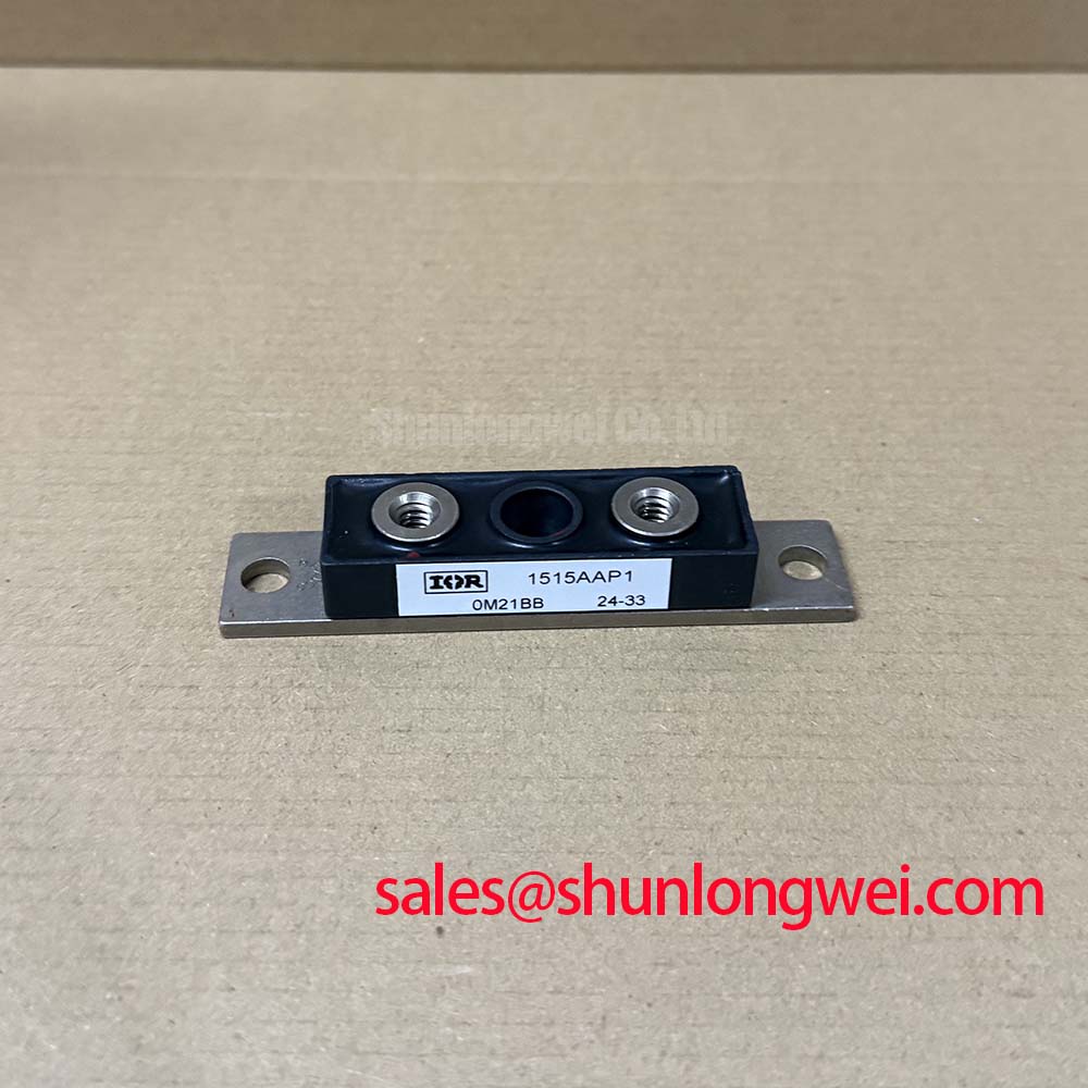
The 1515AAP1 is a highly integrated power management IC developed by Sanken Electric, specifically optimized for high-performance offline switch-mode power supplies (SMPS). This device incorporates a high-voltage power MOSFET and a current-mode PWM controller within a single package, prioritizing board space conservation and reduced component counts. By consolidating the control logic and the power stage, the 1515AAP1 addresses the technical demand for smaller, more efficient AC/DC conversion modules without compromising thermal stability or electrical protection.
- Core Specifications: 650V Drain-Source Voltage | Current Mode PWM | Pulse-by-Pulse OCP
- Engineering Value: Minimizes PCB parasitic inductance by localizing the gate drive loop and reduces external circuitry requirements for startup.
- Addressing Design Challenges: A common question among engineers is how to maintain efficiency at light loads; the 1515AAP1 utilizes frequency reduction or burst mode operation to minimize switching losses during idle states.
Download Official Series Data Reference (PDF)

Technical Analysis: Integration and Thermal Management
The 1515AAP1 distinguishes itself through its robust internal architecture. The integration of a 650V MOSFET ensures a significant safety margin when operating on universal AC inputs (85V to 264V), protecting the silicon from voltage spikes and transient line noise. This high-voltage rating is critical for long-term reliability in environments where input power quality fluctuates. Furthermore, the device utilizes current-mode control, which provides inherent cycle-by-cycle current limiting and simplifies the design of the feedback loop, allowing for faster transient response compared to traditional voltage-mode controllers.
From a thermal perspective, the 1515AAP1 includes an internal Thermal Shutdown (TSD) circuit. To visualize its importance, one can compare the thermal protection to a safety valve on a steam boiler; once the internal junction temperature exceeds the safety threshold, the device halts switching to prevent catastrophic failure, automatically resuming once the temperature settles. This feature, combined with low Rds(on) characteristics of the integrated MOSFET, ensures that the device maintains a cool operating profile even in enclosed adapter housings. For broader system-level protection strategies, engineers often look at coordinated input protection to supplement the IC’s internal safeguards.
Optimized Application Scenarios
This power semiconductor solution is versatile across various low-to-medium power applications. Its design logic is best suited for scenarios where energy efficiency standards (such as Energy Star or ErP Lot 6) are mandatory. The 1515AAP1 is particularly effective in:
- Home Appliance Control Boards: Ideal due to the integrated OVP and TSD, which protect sensitive microcontrollers from power stage failures.
- External AC Adapters: The small footprint and low standby power consumption meet strict global efficiency regulations for consumer electronics.
- Industrial Auxiliary Power Supplies: Suitable for creating stable low-voltage rails from high-voltage DC buses, benefitting from the device’s 650V breakdown rating.
- IoT Gateways: Provides a compact power solution that minimizes electromagnetic interference (EMI) through optimized internal switching transitions.
Conclusion: The 1515AAP1 is best matched for designs requiring under 20W of output power where component density and standby efficiency are primary KPIs.
Key Specifications Table
| Parameter Group | Feature / Rating | Typical Value |
|---|---|---|
| Absolute Maximums | Drain-Source Voltage (Vdss) | 650 V |
| Vcc Input Voltage | 32 V | |
| Electrical Characteristics | PWM Frequency | Fixed (Series Dependent) |
| Startup Current | Low (mA range) | |
| Protection Features | Overload Protection (OLP) | Auto-Restart |
| Thermal Shutdown (TSD) | 150°C (Typical) | |
| Overvoltage Protection (OVP) | Latch/Auto-Restart |
Engineer’s FAQ
Q1: How does the 1515AAP1 improve EMI performance compared to discrete designs?
A1: By integrating the MOSFET and driver, the physical distance between the gate drive and the power switch is virtually eliminated. This minimizes the “loop area” that typically acts as an antenna for high-frequency noise, simplifying the design of the EMI filter.
Q2: What is the recommended startup procedure for this IC?
A2: The 1515AAP1 typically requires a startup resistor connected to the AC line or the rectified bulk capacitor. The internal startup circuit charges the Vcc capacitor until the UVLO-on threshold is reached, at which point the IC begins switching and the auxiliary winding takes over the power supply. For more on modern control, see our guide on software-defined power logic.
Q3: Can this device be used in fanless applications?
A3: Yes, provided the thermal design accounts for the Rds(on) of the MOSFET and the ambient temperature. The internal TSD provides a fail-safe, but proper heat sinking (through PCB copper or external sinks) is recommended to prevent the device from entering protection mode during normal operation.
Professional Summary
The 1515AAP1 is a specialized solution for engineers seeking to balance high integration with rigorous protection standards. By combining a 650V power MOSFET with a precise PWM control stage, this IC enables the development of compact and efficient power supplies suitable for the modern consumer and industrial landscape. Its focus on reducing standby power and simplifying the BOM makes it a predictable and reliable choice for next-generation SMPS projects.