
It’s well-known that operating frequencies for wireless and even wired circuits are rapidly moving up the spectrum, and the corresponding dimensions are shrinking. The reality is that while it wasn’t long ago that operating at just a gigahertz (GHz) or two was considered a test-bench accomplishment but not a mass-production possibility, we now have mass-market consumer products designed for the multi-GHz range and moving up fast with 5G. The physical implications are also well known as frequencies increase and wavelength shrink, so do the associated dimensions and allowable tolerances of components, board tracks, interconnections…well, just about everything.
At these tiny dimensions, making and using even basic components such as connectors is a major challenge, typified by coaxial cables having diameters on the order of a millimeter or two. Connectors and waveguides always had tight dimensional tolerances and the need for some ruggedness. The problem, however, is now aggravated as previously “lesser” or ignorable issues such as surface finish and smoothness can significantly affect the performance of connectors, circuit-board laminates, and more. Fabricating surfaces and connectors at these dimensions are, in many ways, a non-silicon, all-metal version of MEMS (microelectromechanical systems).
At the same time, we’re all aware of how stereolithography (SLA), also called 3D printing or additive manufacturing (AM), has dramatically changed the strategies and actual fabrication associated with mechanical components. This technique, primarily done using various resins or powdered metals, allows for experimental one-off manufacturing, pilot runs, and even medium-volume production runs of parts that would be difficult and even impossible to create via traditional processes and techniques.
Researchers and commercial vendors are now investigating how to use 3D printing to solve gigahertz-range RF challenges. It is being used to fabricate tiny connectors and other components where conventional precision machining or etching is running into barriers. This is especially the case in low-to-moderate volumes where the set-up and tooling effort and cost are relatively high, yet the volume can’t justify costly dies, molds, fixtures, and whatever else it takes to make these minute devices with the dimensional precision and finish needed.
Start with an active 3D-printed GHz device
But why stop with passive devices? One very interesting example of an active device with integral waveguides — the essential interconnect that transitions RF energy to and from an active component — is from a team at the University of Birmingham (UK). They designed and fabricated a 62.5 GHz to 125-GHz Schottky-diode frequency doubler (yes, that’s 125 GHz, not 12.5 GHz) with a split-block waveguide structure using a high-precision SLA printing process (see Reference 1 for their published paper).
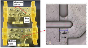
This millimeter-wave IC (MMIC)-like waveguide cavity and flanges were printed using a system from Boston Micro Fabrication (BMF), which uses projection micro stereolithography (PμSL) technology (Figure 1 and Figure 2); you can see more about how this system works in the short BMF video (Reference 2).


Figure 1. Configuration of the 125-GHz frequency doubler showing (a) layout of one split-block; (b) close-up picture of the Schottky-diode MMIC (Image: University of Birmingham).


Figure 2. Picture of the as-fabricated polymer waveguides made by the SLA process (left) and an optical microscope image of the area where the MMIC sits (right) (Image: University of Birmingham).
The printed polymer waveguide parts were plated with copper and a thin protective layer of gold. They characterized the surface roughness of the printed waveguide parts and measured the critical dimensions, and the data showed good printing quality as well as a dimensional accuracy that meets the tight tolerance requirements for such a sub-terahertz active device (Figure 3).


Figure 3. Pictures of the fabricated frequency doubler, showing (a) the fabricated MMIC placed in the 3D-printed waveguide split block and (b) the assembled doubler (Image: University of Birmingham).
Their doubler, which they claim is the first ever produced using SLA, consists of a 20-μm thick GaAs Schottky-diode monolithic microwave integrated circuit (MMIC) fabricated in the waveguide. It has a maximum output power of 33 mW at 126 GHz with an input power of 100 mW, while peak conversion efficiency (an important figure of merit) is about 32% with input powers from 80 to 110 mW.
Schottky diode “refresher”
If you are unfamiliar with using a Schottky diode as a frequency multiplier, the approach uses the common technique of employing a non-linear element — here, a diode — to create harmonics when driven by a fundamental frequency waveform (Figure 4).


Figure 4. (top) The block diagram of the frequency doubler using a non-linear element; (bottom) the core schematic of that frequency doubler (Image: QSL.net).
Of course, for GHz-range work, the simple schematic can only a hint at what it really takes to build a doubler in practice, as those simple lumped elements in the schematic diagram have a very different manifestation in the gigahertz reality than what is indicated by those simple symbols in the line drawing.
Using precision SLA and the materials it supports opens a new path for creating unique high-GHz passive and active components for custom, low-volume, and perhaps even higher-volume applications. The approach may allow for fabricating these components using designs and arrangements which would be difficult if not impossible to do using conventional techniques. It may also bring new meaning to the concept and implementation of an integrated gigahertz-class component.
Next stop: Terahertz waves
While devices for the range of multi-tens to hundreds of gigahertz range are very difficult to fabricate and interconnect, those for terahertz (THz) waves are in another realm of difficulty. One THz is formally equal to 1000 GHz, and the terahertz band is generally considered to include frequencies between 100 GHz and 10 THz, corresponding to wavelengths between 3 millimeters and 30 micrometers.
Even though the terahertz frequencies represent electromagnetic energy and are governed by Maxwell’s well-known equations, this band presents a unique set of component and design dilemmas. Devising components — especially active ones — for this band to provide gain and other necessary functions switching, is almost like an exercise in magic coupled with art.
Why so? To put it in relatively simple terms, terahertz frequencies are too high for active electronic devices because of excessive loss and limited carrier velocity, but they are too low for photonic devices because of the lack of materials delivering a sufficiently small bandgap (Reference 3).
For these and other reasons, “3D printing” and “terahertz waves” are not phrases you would expect to see in the same sentence, but they can be made to work together. Researchers at Philipps-Universität Marburg (Germany) and Centro de Investigaciones en Óptica, A.C. (León, Mexico) worked together to create a 3D-printed diffraction grating that can be used to reflect and steer terahertz waves. They “printed” a reflective diffraction grating starting with a one-dimensional array of 17 plastic strips, each 50 mm long and 0.8 mm wide, covered this with aluminum foil, and then connected them by V-shaped springs (Figure 5).


Figure 5. The 3D-printed grating is an accordion-like panel with a thin aluminum layer for reflecting the impinging electromagnetic radiation (Image: Philipps-Universität Marburg).
The adjustable grating was then mounted in a vise, also 3D-printed, and used to apply pressure to adjust the dimensional spacing of the strips (Figure 6). The array period was 2.3 mm when relaxed but could be continuously reduced to 1.1 mm by applying lateral pressure via the vise action.


Figure 6. The grating is mounted in a 3D-printed vise, which can precisely compress the folds to adjust the spacing and periodicity of the rows and, thus, the grating’s spectral characteristics (Image: Laser Focus World).
Tests over the range of 0.1 to 1 THz showed the device’s usefulness for steering a terahertz beam through angles of 25° or greater. To measure the grating’s performance, they created a data set using terahertz waveforms with detector-arm angles between 30° and 55° in 0.5° steps (Figure 7).


Figure 7. (a) Photograph of the free-standing grating as printed; (b) Photograph of the grating in its pressing mount, a close-up image of three periods of the grating with a reference scale on the right-hand-size (1 mm per line) is provided; (c) Schematic of geometry of the THz optical path, the receiver and its corresponding lens are mounted on a motorized goniometer to vary the detection angle (Image: Philipps-Universität Marburg/Centro de Investigaciones en Óptica, A.C.).


Figure 8. (a) The spectra obtained for angles between 30° (lighter color) and 55° (darker color) in 0.5° steps for the grating compression with a period of 2.92 mm. The spectral peak clearly shifts as a function of the detection angle as indicated by the arrow; on the right-hand side, additional peaks can be seen, which correspond to the second diffraction order; (b) and (c) show analogous sets of spectra for compressions with a period of 2.52 mm and 2.11 mm respectively; notice that the collection of spectral peaks for the first-order diffraction appear at higher frequencies as the period decreases; (d) The peak frequency of all the spectra shown in panels (a)= □, (b)= ◯ and (c)= △ are plotted here. The continuous lines represent the relation between the frequency and the angle of the first-order diffraction (Image: Philipps-Universität Marburg (Germany)/Centro de Investigaciones en Óptica, A.C.(Mexico)).
The compression on the grating was increased (decreasing the periodic spacing of the grating) with the measurements repeated with three different compressions (Figure 8); the results were obtained by Fourier transformation of the waveforms.
The research project did not stop with testing of this basic arrangement, as they also decided to test the possibility of “active” beam steering using a different arrangement. They 3D-printed a larger grating optimized for 120-GHz operation and placed it in a mount, and then they fixed and coupled the ensemble to an audio speaker. By doing so, the oscillations from the speaker were able to impose a compression/decompression motion on the grating.
The speaker was driven by a 60.5-Hz sine wave (chosen due to mechanical resonance issues, not the AC-line frequency), and they were able to see the impinging continuous-wave (CW) THz beam being steered forwards and backward while being synchronized to the speaker motion. Full details on both parts of the project are in (Reference 4).
Related EE World Content
Why 3D packaging could be the next breakthrough for processing
How are sensors used in 3D bioprinting?
3D printing for 5G systems
3D printing and bacteria blend for solar harvesting
What are the applications of 3D and 4D printed electronics?
External References
IEEE Transactions on Terahertz via University of Birmingham (UK), “125 GHz Frequency Doubler using a Waveguide Cavity Produced by Stereolithography”
Boston Micro Fabrication, “Learn How PµSL Works”
Microwave Journal., “THz Generation and Analysis with Electronic and Photonic Technologies”
OSA Optics Express, “Terahertz beam steering using active diffraction grating fabricated by 3D printing”.