Mitsubishi CM1000DUC-34SA: A 1700V 1000A Dual CSTBT IGBT Module for High-Power Applications
CM1000DUC-34SA Mitsubishi 1700V 1000A Dual CSTBT IGBT Module
The CM1000DUC-34SA is a dual CSTBT™ power semiconductor module rating at 1700V and 1000A, manufactured by Mitsubishi Electric. It features advanced carrier-stored trench-gate technology to minimize conduction losses in megawatt-class power conversion systems. Engineers seeking to optimize efficiency in high-power applications can leverage this dual-switch configuration to manage heat generation and reduce footprint requirements.

Key Specifications
- Collector-Emitter Voltage (Vces): 1700V
- Collector Current (Ic): 1000A
- Collector-Emitter Saturation Voltage (Vce(sat)): 2.20V (typical at Tj = 125°C)
Key Advantages
- Reduced Conduction Losses: CSTBT™ technology lowers Vce(sat) compared to traditional trench gate architectures.
- Integrated Thermal Protection: Features a built-in NTC thermistor for precise, isolated junction temperature monitoring.
Download Official Datasheet (PDF)
Technical Analysis Around Unique Value Proposition
The core value of the CM1000DUC-34SA lies in its carrier-stored trench-gate bipolar transistor (CSTBT™) technology. This structure increases carrier density near the emitter side. Consequently, it achieves a lower collector-emitter saturation voltage without increasing switching losses. This optimization directly addresses the classic trade-off in power semiconductors, helping designers maintain system efficiency under heavy thermal loads.
Thermal management is supported by an isolated copper baseplate. The junction-to-case thermal resistance ($R_{th(j-c)}$) is rated at a low 0.017 K/W for the IGBT portion. You can think of thermal resistance like a highway lane width. A lower resistance value provides a wider path, letting thermal energy flow away from the silicon die to the heatsink without bottlenecking. This performance decreases the thermal stress on internal bond wires during power cycles.
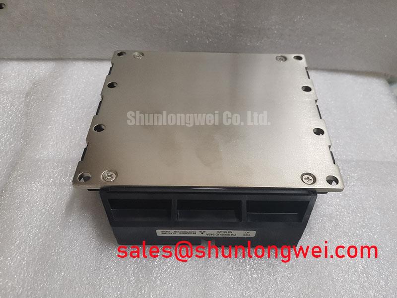

Minimizing stray loop inductance is critical in high-current applications. The symmetric terminal arrangement of this module helps mitigate parasitic voltage spikes during high di/dt switching transitions. Integrating this layout alongside optimized gate drivers limits voltage overshoots, reducing the requirement for large, complex snubber circuits.
Optimized Application Scenarios
- Wind Power Converters: High current density and robust thermal cycle limits make this module suitable for grid-tied wind turbine systems.
- Utility-Scale Solar Inverters: Lower conduction losses maximize total energy output under varying solar irradiation levels.
- Industrial Motor Drives: The module supports heavy startup currents and benefits from thermal tracking via the integrated NTC.
This module matches high-power industrial applications requiring efficient thermal dissipation and low conduction loss profiles.

Key Specifications Table
| Absolute Maximum Ratings (Tc = 25°C unless otherwise specified) | ||
|---|---|---|
| Collector-Emitter Voltage | Vces | 1700 V |
| Gate-Emitter Voltage | Vges | ±20 V |
| Collector Current (DC) | Ic | 1000 A |
| Maximum Junction Temperature | Tjmax | 150 °C |
| Electrical Characteristics (Tj = 25°C unless otherwise specified) | ||
| Collector-Emitter Saturation Voltage | Vce(sat) (at Ic = 1000A, Vge = 15V) | 2.20 V (typ, Tj = 125°C) |
| Gate-Emitter Threshold Voltage | Vge(th) (at Ic = 100mA) | 6.0 V – 7.5 V |
| Thermal Resistance (Junction-to-Case) | Rth(j-c) (IGBT, per 1/2 module) | 0.017 K/W |
Engineer FAQ
How does CSTBT™ technology improve efficiency in the CM1000DUC-34SA?
CSTBT™ technology introduces a carrier storage layer. This layer increases the density of charge carriers in the drift region during conduction. As a result, it reduces the forward voltage drop (Vce(sat)), lowering total conduction losses without raising switching energy penalties.
What is the benefit of the integrated NTC thermistor in this module?
The integrated NTC thermistor provides direct thermal monitoring close to the silicon chips. This close proximity reduces response lag compared to external case-mounted sensors. It allows control circuits to implement real-time thermal derating protection, preventing thermal runaway.
How does packaging design address parasitic inductance in this module?
The module package utilizes low-profile, symmetric power terminals to balance current distribution. This layout reduces internal loop area, which helps control parasitic inductance and voltage spikes during turn-off phases.
What is the insulation voltage rating of the CM1000DUC-34SA?
The module features an isolation voltage rating of 4000 Vrms (AC, 1 minute, 50Hz/60Hz) between the terminals and the baseplate, meeting common industrial isolation standards.
Conclusion
The CM1000DUC-34SA dual IGBT module delivers high-current density and optimized conduction performance within a robust mechanical package. By leveraging CSTBT™ technology and low thermal resistance baseplate designs, this device enables engineers to design compact, high-efficiency power conversion topologies in the power semiconductors field.