Infineon FZ900R12KE4HOSA1 1200V 900A Single IGBT Module: A Technical Overview
FZ900R12KE4HOSA1 Infineon 1200V 900A Single IGBT Module
Introduction and Core Highlights
The FZ900R12KE4HOSA1 is a high-power single IGBT module designed by Infineon to deliver robust switching performance. It integrates Trenchstop™ IGBT4 technology with an Emitter Controlled diode to optimize power conversion efficiency in heavy industrial systems.
- Core Specifications: 1200V Collector-Emitter Voltage | 900A Continuous DC Collector Current (at Tc = 80°C) | 10µs Short-Circuit Withstand Time.
- Key Benefits: Low saturation voltage minimizes conduction losses, and high thermal cycling capability extends operating lifetimes.
For power electronics engineers, managing transient voltage spikes during high-current switching is critical to preventing device failure.
Download Official Datasheet (PDF)

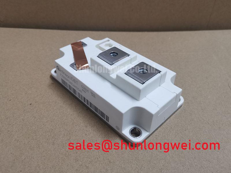
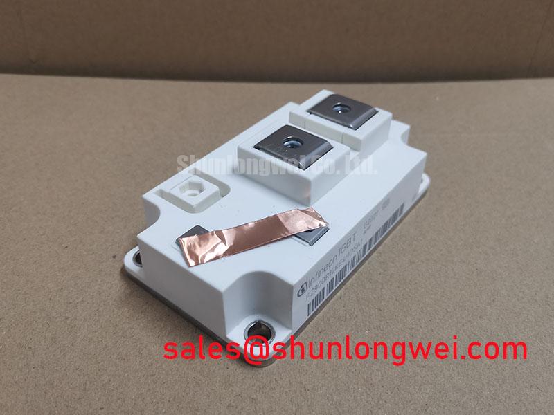
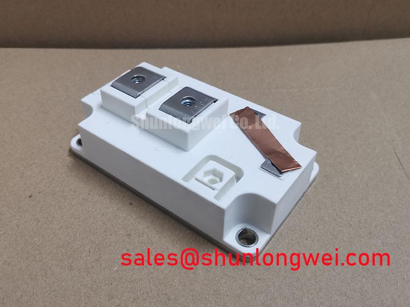
Technical Analysis of the Trenchstop™ IGBT4 Architecture
Trenchstop™ IGBT4 technology represents a major shift in power semiconductor design, addressing the historical trade-off between switching speed and conduction losses. For a deeper look at this tech, consult this guide on decoding IGBT4 architecture. The FZ900R12KE4HOSA1 exhibits a typical collector-emitter saturation voltage (VCE(sat)) of 1.70V at its rated current. This low conduction barrier keeps power loss to a minimum during the on-state.
Thermal dissipation is managed via an isolated copper baseplate. The thermal resistance from junction to case (RthJC) for the IGBT portion is rated at 0.071 K/W. Think of thermal resistance as a narrow highway during rush hour. A lower resistance value provides more lanes, allowing heat to escape quickly to the heatsink. This keeps the junction temperature below the maximum limit of 150°C under continuous load. To model these thermal dynamics, reference this guide on IGBT thermal design and Zth curves.
Gate control characteristics are highly optimized in this module. The typical input capacitance (Cies) is 57 nF, which demands robust gate drive circuitry. Managing the gate charge displacement helps prevent spurious turn-on events. Utilizing silicone gel insulation inside the module housing protects the chip layout from high voltage transients and environmental moisture.
Optimized Application Scenarios
- High-Power Industrial Inverters: The 900A current rating enables efficient motor control inside large variable speed drives.
- Solar Inverter Central Stages: The 1200V voltage class aligns with standard utility-scale DC bus configurations.
- Uninterruptible Power Supplies (UPS): Fast switching speeds and low losses ensure reliable backup power conversion.
- Wind Turbine Power Converters: Robust short-circuit withstand capabilities protect the converters during grid transients.
The FZ900R12KE4HOSA1 is the optimal choice for megawatt-range inverters requiring low conduction losses and high short-circuit survivability.
Key Specifications Table
| Absolute Maximum Ratings (Tj = 25°C unless otherwise specified) | ||
|---|---|---|
| Collector-Emitter Voltage | VCES | 1200 V |
| Continuous DC Collector Current | IC (Tc = 80°C) | 900 A |
| Repetitive Peak Collector Current | ICRM (tp = 1 ms) | 1800 A |
| Gate-Emitter Peak Voltage | VGES | +/- 20 V |
| Electrical Characteristics (Typical Values) | ||
| Collector-Emitter Saturation Voltage | VCE(sat) (IC = 900A, Tj = 125°C) | 2.00 V |
| Gate Threshold Voltage | VGE(th) (IC = 33mA, Tj = 25°C) | 5.8 V |
| Input Capacitance | Cies (f = 1 MHz, VCE = 25V) | 57 nF |
| Short-Circuit Withstand Time | tsc (VGE ≤ 15V, VCC = 800V, Tj = 150°C) | 10 µs |
Engineer FAQ
Q1: How to manage thermal dissipation in high-power IGBT configurations using the FZ900R12KE4HOSA1?
A1: Keep thermal contact resistance minimal by applying high-performance thermal interface material (TIM) between the module copper baseplate and the heatsink. Ensure the mounting torque is strictly within the specified 3.0 to 6.0 Nm range to maintain uniform contact pressure.
Q2: What is the short-circuit capability of this module?
A2: The module features a short-circuit withstand time (tsc) of 10 microseconds under worst-case conditions (VGE ≤ 15V, VCC = 800V, Tj = 150°C), allowing protection circuits sufficient time to trigger shutdown.
Q3: Why is the input capacitance value of 57 nF significant for gate driver design?
A3: A high input capacitance requires the gate driver to supply sufficient peak current to quickly charge and discharge the gate. Proper design prevents prolonged switching times that increase switching losses. To learn more about transition phases, read about switching transients and the Miller plateau.
Conclusion
The FZ900R12KE4HOSA1 represents a reliable solution for high-power switching applications. By balancing low conduction losses with structural robustness, it allows engineers to achieve compact, thermally efficient designs without compromising system safety.