Precision 15Msample/s data acquisition module for hardware-in-the-loop
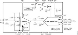
Called ADAQ23875, it has differential input signal conditioning circuitry including 0.005% matched resistors to implement a ±2.048V input range with a 4.096V reference – the reference is also included but can be over-driven from outside.
Important parameters are:
- ±0.4 LSB typical INL (±1 LSB max)
- 89dB typical SINAD at 1kHz
- -115dB THD at 1 kHz (-106dB at 400kHz)
- 0.005% FS typical gain error
- ±1ppm/°C max gain error drift
- -40°C to +85°C operation
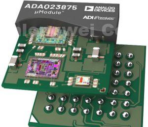 All this comes in a 9 x 9mm BGA (100 ball, 0.8mm pitch).
The converter inside is a successive approximation type with typically 58ns between conversion initiation and data availability.
Single 5V supply operation is possible (±2.048V input range), according to the company, although this does not account for the 2.5V (40mA) rail called for by the data sheet for the input-output circuitry – LVDS (low voltage differential signalling) is used for the interface with one-lane or two-lane output modes.
Other supplies needed are 5V (4.6mA) for the internal logic, then a maximum of 10V between the positive (+5V 4mA nominal) and negative (0V 4mA nominal) analogue rails.
Power consumption is typically 143mW at 15Msample/s.
An evaluation board is available.
The ADAQ23875 only has precision input resistors for one input range, while two product in the pipeline (sampling now) have five possible modes: ±10, ±5, ±4.096, ±2.5 or ±1.5V.
16bit ADAQ23876 planned for August
18bit ADAQ23878 planned for September
Other applications are foreseen in mass spectrometry, medical imaging and ultrasonic flow meters.