An In-Depth Look at the STMicroelectronics STE07DE220 Monolithic ESBT Module
STE07DE220 STMicroelectronics Monolithic ESBT Module
Introduction and Core Product Highlights
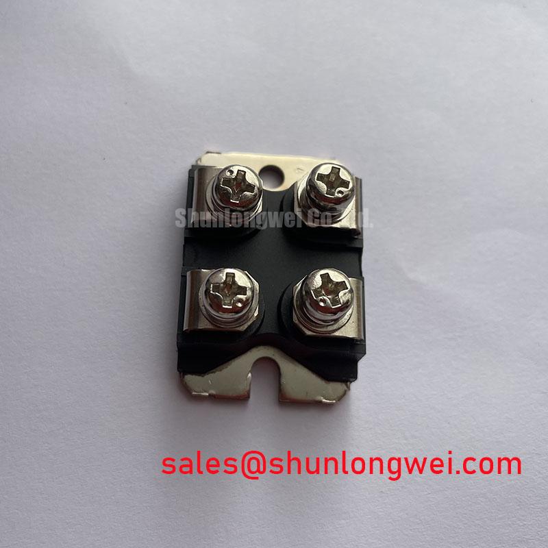
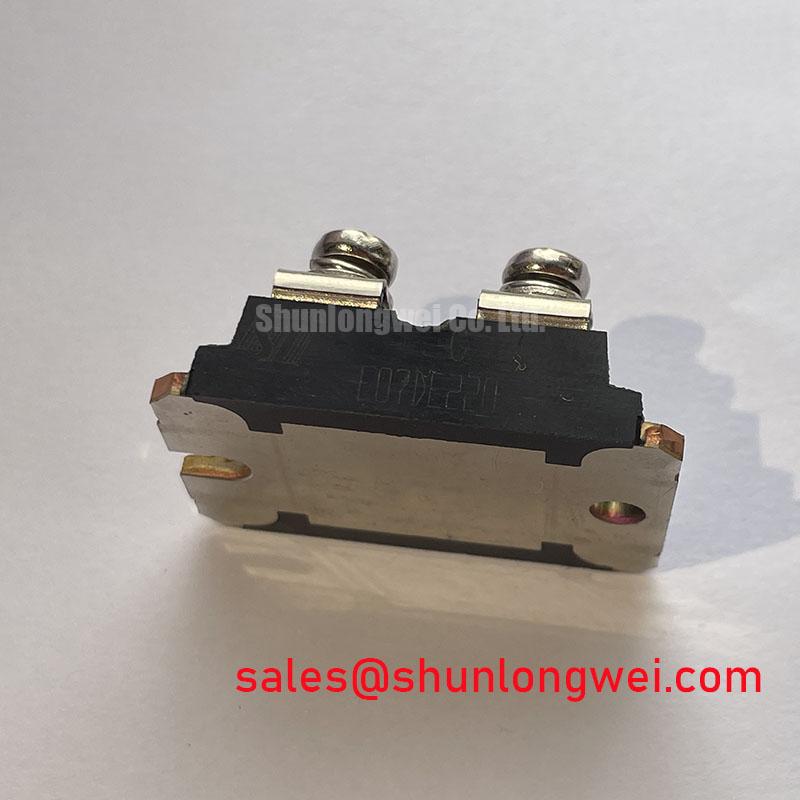
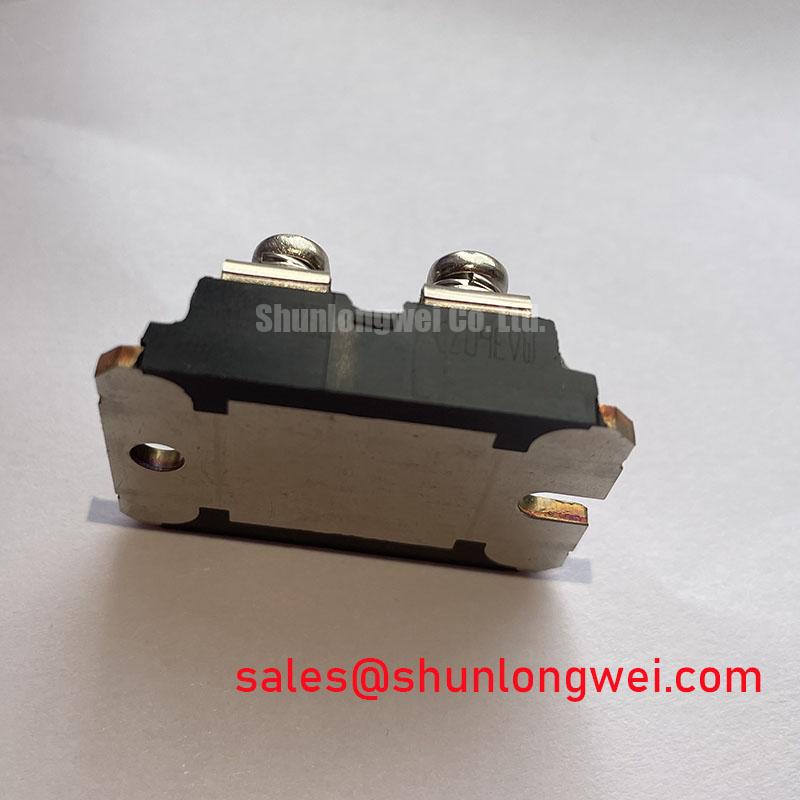
The STMicroelectronics STE07DE220 is a monolithic Emitter Switched Bipolar Transistor (ESBT) housed in an ISOTOP package. It integrates a high-voltage bipolar transistor and a low-voltage power MOSFET in a cascode configuration to deliver a 2200V blocking voltage and a 7A continuous collector current. This device addresses the requirement for ultra-high voltage switching with low conduction losses, achieving a typical collector-source saturation voltage ($V_{CS(sat)}$) of just 0.9V. This integration helps engineers optimize power converter stages in high-voltage environments without using complex series-connected discrete switches.
For more design details, you can download the official STE07DE220 datasheet (PDF).

Technical Analysis of the Cascode Architecture
The cascode structure of the STE07DE220 resolves a historical trade-off in power design: the conflict between high-voltage blocking capability and fast switching speeds. In a traditional high-voltage bipolar transistor, switching speed is constrained by the minority carrier storage time in the base region. By placing a low-voltage MOSFET in series with the emitter of the high-voltage bipolar transistor, the emitter current is abruptly interrupted during turn-off. This configuration forces the collector current to flow out of the base terminal, accelerating charge extraction and reducing switching losses.
To understand this switching mechanism, think of it as a high-pressure water main controller. Instead of slowly turning off a large, heavy high-pressure valve, a fast-acting gate valve is slammed shut right at the outlet. This immediately stops the main flow, preventing leakage and tail currents. Consequently, the STE07DE220 exhibits a square reverse biased safe operating area (RBSOA) up to its maximum 2200V rating. This robustness is critical for preventing thermal runaway during hard switching transients, which is a common issue analyzed in our IGBT failure analysis guide.
The device is positioned alongside alternative technologies detailed in the IGBT vs SiC vs GaN comparison. The package provides an internal ceramic insulation layer, delivering a minimum isolation voltage of 2500 V RMS between the active terminals and the baseplate. This simplifies the physical mounting layout on the heatsink while maintaining electrical isolation safety.

Target Application Scenarios
- Three-Phase Auxiliary Switch-Mode Power Supplies (SMPS): The 2200V blocking voltage accommodates wide input DC bus variations from rectified 400V/480V AC mains without requiring snubbers or series transistors.
- Industrial Active Power Factor Correction (PFC): Low conduction loss ($V_{CS(sat)}$ of 0.9V at 7A) maintains high efficiency in continuous current mode converters.
- High-Voltage Capacitor Charger Circuits: The square RBSOA ensures reliability during repetitive, pulse-like charging phases that stress the safe operating area boundaries.
- Uninterruptible Power Supplies (UPS): Monolithic construction minimizes component count, improving system MTBF in backup power switchboards.
Best Match: The STE07DE220 is optimal for auxiliary power supplies operating off three-phase industrial grids requiring a single-switch 2200V topology.
Key Specifications Parameter Table
| Parameter | Symbol | Value | Unit |
|---|---|---|---|
| Absolute Maximum Ratings | |||
| Collector-Source Voltage (V_BE = 0) | V_CS(SS) | 2200 | V |
| Collector-Emitter Voltage (V_BS = 0) | V_CE(active) | 2200 | V |
| Continuous Collector Current (Tc = 25°C) | I_C | 7 | A |
| Total Power Dissipation (Tc = 25°C) | P_tot | 100 | W |
| Electrical Characteristics (Tj = 25°C unless noted) | |||
| Collector-Source Saturation Voltage (Ic = 7A, Ib = 1.4A) | V_CS(sat) | 0.9 (typ) | V |
| Gate Threshold Voltage (V_DS = V_GS, Id = 250µA) | V_GS(th) | 2.5 to 4.5 | V |
| Thermal Characteristics | |||
| Thermal Resistance, Junction-to-Case | R_thj-case | 1.25 | °C/W |
Engineer FAQ
How does the cascode configuration of the STE07DE220 improve efficiency in power supplies?
The cascode design bypasses the slow turn-off characteristics of high-voltage bipolar transistors by using a low-voltage MOSFET to interrupt the emitter current. This layout minimizes minority carrier storage time, reducing switching losses and allowing higher operating frequencies.
What are the drive requirements for the base and gate terminals?
The device requires base current control for conduction, combined with voltage control at the gate terminal to handle emitter switching. Refer to the datasheet timing diagrams to properly coordinate base current ($I_B$) injection with gate-source voltage ($V_{GS}$) transitions.
How should the thermal interface for the ISOTOP package be designed?
Ensure a maximum junction-to-case thermal resistance ($R_{thj-case}$) of 1.25°C/W by applying high-performance thermal interface material. Tighten the mounting screws to the specified torque to maintain uniform pressure across the internal alumina substrate.
Designing for High-Voltage Switch-Mode Topologies
The STE07DE220 combines the high-voltage capability of a bipolar junction transistor with the rapid switching control of a modern MOSFET. This cascode integration simplifies driver architectures and reduces cooling footprint constraints, helping design engineers achieve stable conversion stages in high-voltage industrial applications in our power semiconductors portfolio.