The dramatic rise in manufacturing test time for today’s large and complex SoCs is rooted in the use of traditional approaches to moving scan test data from chip-level pins to core-level scan channels. The pin-multiplexing (mux) approach works fine for smaller designs but can become problematic with an increase in the number of cores and the design complexity on today’s SoCs. The next revolution in DFT tools to take test time, test cost, and DFT implementation effort eliminates the challenges of pin-mux approach by decoupling the core-level DFT requirements from the chip-level test delivery resources.
Challenges of the pin-muxed approach
A common way to connect core-level scan channels to chip-level pins is by using a mux network to determine which cores are connected to chip-level pins. This works fine for smaller designs, but becomes problematic as the number of cores grows, the levels of hierarchy increase, and designs become more complex. It presents barriers to efficiently testing cores in parallel to save on time and cost. Challenges include:
- Limited IOs available for scan test
- Limited channels at the core level
- Test configurations fixed during the design process
- Potential for routing congestion from additional scan channels
In a bottom-up DFT approach, DFT engineers typically allocate a fixed number of scan channels for each core early in the flow, usually the same number for each core. This is the easiest approach, but it can end up wasting bandwidth because the different cores that are grouped together for testing might have different scan chain lengths and pattern counts (fig. 1).


Figure 1. In a hierarchical DFT flow, putting less effort into the mux network can lead to sub-optimal bandwidth usage.
Another approach that reduces wasted bandwidth issue and saves test time is to reallocate scan resources once required data per core is known, but doing so involves reconfiguring compression, rerouting the scan channels, and regenerating patterns (fig. 2).


Figure 2. Building a more complex mux network to better align scan channel input and outputs will save test time, but at the cost of implementation effort.
Is the additional effort worth the savings in test time? Each DFT team must decide on these tradeoffs. For designs with more complex hierarchical strucutres, large numbers of identical cores, or layout with tiling, additional challenges and tradeoffs have to be overcome.
Streaming Scan Network approach
A new approach to distributing scan test data across an SoC—called Streaming Scan Network (SSN)— reduces both DFT effort and test time, with full support for tiled designs and optimization for identical cores. The SSN approach is based on the principle of decoupling core-level test requirements from chip-level test resources by using a high-speed synchronous bus to deliver packetized scan test data to the cores.
The number of scan channels per core is independent of the width of the SSN bus and the number of scan channels at chip level and from the number of cores in the design. Delivering test data in this way simplifies planning and implementation and allows core grouping to be defined later in the flow, during pattern retargeting rather than during the initial design. The SSN architecture is flexible—the bus width is determined by the number of scan pins available—and eases routing congestion and timing closure because it eliminates top-level test mode muxing, which also makes it ideal for abutted tile-based designs.
Part of the SSN architecture is the core-level host nodes that generate the DFT signals locally. The host nodes ensure that the right data is picked up from SSN bus and sent to scan inputs of the core and that the output data is placed back onto the bus. Each node knows what to do and when to do it based on a simple configuration step leveraging IJTAG (IEEE 1687) infrastructure. Which groups of cores will be tested together and which will be tested sequentially is configurable, not hardwired, with the SSN approach. The configuration is done as a setup step once per pattern set, and once it’s done, all the data on the SSN bus is payload.
What is packetized scan test data delivery?
As an example, take a design in which two cores are to be tested concurrently using SSN (fig 3). Block A has 5 scan channels, Block B has 4 scan channels. A packet is the total amount of data needed to perform one shift cycle across both cores. The packet size in this example is 9 bits. However, there are 16 pins available for scan test (8 inputs, 8 outputs), so the SSN bus is 8 bits wide.
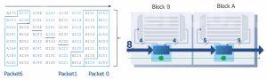

Figure 3. Testing two blocks at the same time. In a pin-mux scan access method, this would require nine chip-level scan input pins and nine scan output pins. With SSN the packet size is 9 bits, which is delivered on an 8-bit bus.
The table on the left side of figure 3 shows how the data is streamed through the synchronous SSN bus to the cores. It will take two SSN bus cycles to deliver all the data required to perform one shift cycle in both cores. Note that the bit location of the data corresponding to each core changes (rotates) for each packet. The host nodes know where the data corresponding to that core resides on the bus and when to generate local DFT signals, including pulsing the core shift clock.
How SSN reduces test time and test data volume
SSN contains several capabilities to reduce test time and test data volume. One is independent shift and capture. In many retargeting schemes, the capture cycles of all the affected cores must be aligned. If multiple cores are shifting in concurrently (fig. 4) and they have different scan lengths, some of the cores with shorter chains need to be padded to perform capture at the same time for all cores. With SSN, the host nodes are programmed so that each core can shift independently, but capture occurs concurrently once all the cores have completed scan load/unload.
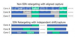

Figure 4. When capture cycles must be aligned, some cores need padding, which is a waste of data and test time.
SSN also performs bandwidth tuning. Rather than providing as many bits as there are core-level scan channels per packet, SSN can allocate fewer bits to a core that requires less data overall. For a core that has fewer patterns or shorter scan chains, less data is allocated per packet, which better distributes the data across the cores and ultimately reduces test time.
SSN is a scalable method for testing any number of identical cores with a constant amount of test data and test time. For identical cores, the compare circuitry is included in each host node. Data provided to the identical cores is scan input, expect data, and mask data. That allows SSN to do a comparison inside each core. The accumulated status across all identical cores is then shifted out on the SSN bus. A pass/fail bit per core is also captured in the host and scanned out through IJTAG.
Summary
SSN was developed in collaboration with several leading Semiconductor companies. We presented a paper with Intel at the International Test Conference 2020 that describes the technology and shows some key results of Intel’s validation of SSN. Compared to a pin-muxed solution, they saw a reduction in test data volume of 43% and also a reduction of test cycles of 43%. Steps in the design and retargeting flow were between 10x-20x faster with SSN.
SSN eliminates the tradeoffs between having an effective, streamlined implementation flow, or minimizing test cost.
Geir Eide is a Product Management Director for the Tessent DFT test products at Siemens Digital Industries Software.