Aldec launches HES board for ASIC & SoC designs

Aldec has launched the HES-VU19PD-ZU7EV, an ASIC/SoC physical prototyping and hardware emulation board that can accommodate designs of about 83M ASIC gates in size.
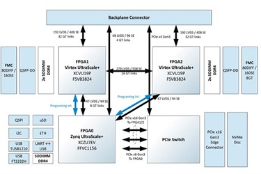
The HES-VU19PD-ZU7EV uses just two FPGAs for the provision of logic which simplifies FPGA partitioning and reduces project bring-up time for designs targeting a medium-sized ASIC or SoC.
For larger designs, four boards can be connected via a high-speed backplane (scheduled for launch later in the year) to provide the equivalent of about 332M ASIC gates. It will also be possible to connect backplanes together (up to three), to cater for designs of about 996M ASIC gates.
The HES-VU19PD-7U7EV’s logic module FPGAs are both Virtex UltraScale+ VU19P devices, Xilinx’s highest logic capacity FPGA to date. The board also features a Xilinx Zynq UltraScale+ ZU7EV MPSoC which acts as the host module and has a quad-core ARM Cortex-A53, dual-core ARM Cortex-R5 real-time processing units and PCIe Gen3 embedded IP.
Commenting Zibi Zalewski, General Manager of Aldec’s Hardware Division, said, “For this new platform we’ve replicated much of the system architecture of our popular dual FPGA boards in our HES-7 family and incorporated the newest and largest UltraScale+ FPGAs from Xilinx to greatly extend the capacity and functionality for both emulation and prototyping scenarios. Also, our use of the Zynq US+ device as a controller, means it can host the testbench for prototyping. Indeed, the prototyping and emulation capabilities of our HES boards is unique to Aldec.”
Zalewski also indicated that a revision to HES-DVM, Aldec’s fully automated and scalable hybrid verification environment for SoC and ASIC designs, is in the pipeline. “That will further unleash the power of the new board, through enhanced debug capabilities, for example,” he added.
The HES-VU19PD-7U7EV has a PCIe Switch device which provides PCIe x16 Gen 3 connections with the logic devices and PCIe x8 Gen 3 connections with the controller FPGA.
Other interfaces include QSFPDD on each of the logic FPGAs and Ethernet (1Gb) and USB on the control FPGA.
In terms of interfacing with memory, the board provides five SODIMMs for accommodating external DDR4 memory (two per VU19P and one for the ZU7EV) plus NVMe M.2 PCIe for additional SSD storage.
The HES-VU19PD-7U7EV is supplied with Aldec’s HES Proto-AXI software package which includes all necessary drivers and utilities for communicating with and programming the board. For quick bring-up of the host connection, Aldec provides a ready-to-use image of the embedded Linux for the ZU7EV device.